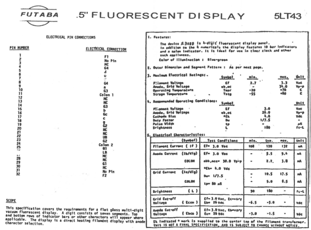
I'm no stranger to designing and building clocks. I must have made a good 20 so far. (LED, LCD, Nixie) But this VFD is killing me! It's a 4 digit FUTABA VFD. I have the datasheet, so I know all the pinouts.
I picked up a 28 pin TSSOP breakout and soldered the MAX6921 to it so that I could put it on my breadbaord. I'm powering the VFD with a 25V boost converter. And I have 3V on the filaments. I understand how to power it. No problems there. I'm having trouble wrapping my head around driving it with a MAX6921.
I've tried a few code snippets and examples but I can't for the life if me get this display to do anything. A lot of the code examples that I'm finding are for the 8-digit IV-18 tubes. I've tried to modify the code, but the most I managed to do was to get one segment to light up. And I'm not even sure why it's doing that.
I'm having trouble understanding how to designate the 20 outputs on the MAX6921 to be the grids and the segments. I must be missing something fundamental.
Does anyone have a code example that will just work? I don't even need clock code. That I can figure out. In order to understand the code, I need to know how to get it to do something simple like just display a static number. After that, it'll be easy to get it to display numbers from a RTC.
See Figure 4 of the data sheet for the required signals.
For testing purposes you can pulse LOAD after every CLK pulse, and a delay, so that you can see whether the data is shifted and latched as expected.
Even if you are confident to have connected everything properly, a circuit diagram would be helpful. As you stated, you must have missed something fundamental.
But there are 20 outputs on the 6921. How do you know what goes where? How do you determine what outputs go to the grids and what go to the segments?
I'd think it would be something like OUT0-OUT3 would be from grids 1, 2, 3, and 4 and OUT4-OUT10 would be for A, B, C, D, E, F, G. But how is that specified in the code?
Yes, the FUTABA datasheet above is from my site. The pinouts on the display is not the problem, or figuring out how to power it. It's figuring out how to tell the 6921 what pin is what. The data sheet says that OUT0-OUT19 are "VFD Anode and Grid Drivers. OUT0 to OUT19 are push-pull outputs swinging from VBB to GND". So it sounds like all the pins are the same. It's not like on a LED driver where they are 'a', 'b', 'c', etc. How do I know what goes to the grids, and what goes to the segments? And how do you distinguish that in the code?
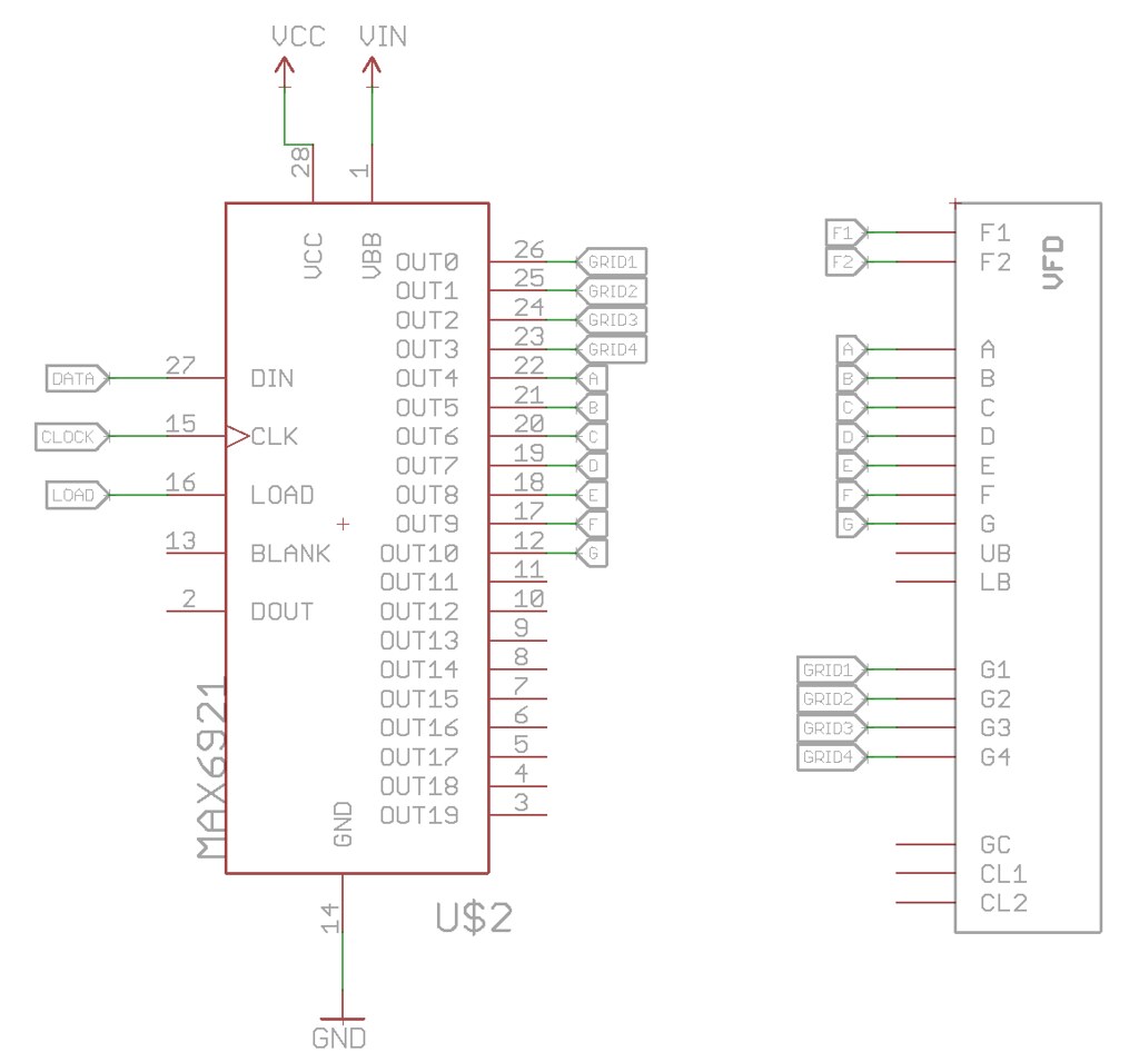
My schematic looks like this so far. And all the code samples I've found for the 8-digit IV-18 that I attempted to modify for 4 characters doesn't seem to do anything.

