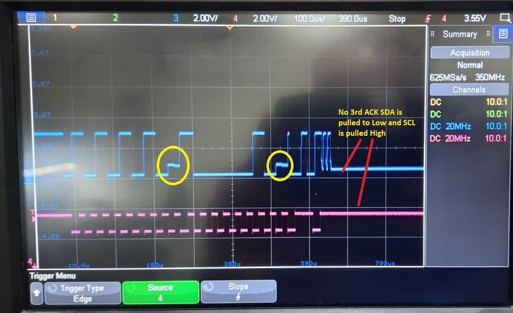
Nothing in that picture is expected behavior
The low ACK level by the Slave is too high, the Master might not see it as a valid ACK. It looks like a shortcut on the I2C bus.
The Master is sending bytes, but after two bytes, there is a extra SCL low pulse. That does not make sense, unless the Master detects a bus collision.
The last pulses of SDA are too short, that does also not make sense.
Start with the I2C bus with a I2C Scanner sketch. It should be reliable and the signals should be normal I2C bus signals.
Which Arduino board do you use as the Master ?
Can you tell what the protocol is for the DUT, can we read that somewhere ?
Can you show the sketch ?
What else is connected to the I2C bus ? Other devices ? Pullup resistors ? Did you connect the GNDs of the Master and the Slave ?
Do you use a I2C level shifter ?
What kind of wires do you use for the I2C bus ? Can you show a photo so we can see the wires ? SDA should not be next to SCL in a cable, especially not in a flat-ribbon cable.
These ACK levels indicate that your slave Device (Under Test) can not provide a proper LOW level. It seems to be confused and finally pulls SDA permanently low what again can confuse the master.
Read carefully what @Koepel wrote about possible problems with your circuit.
What is a DUT ? DUT IS MY COMPANYS ASIC WHICH WILL BE USED INSIDE A MEMS Microphone.
Which Arduino board do you use as the Master ? Arduino nano
Can you tell what the protocol is for the DUT, can we read that somewhere? No Companys IP
Can you show the sketch ?Yes
What else is connected to the I2C bus ? Other devices ? Pullup resistors ?:Only DUT is connected,pullup can be seen in the skectch.We are using 10K.
Below wave from is captured when read is happening properly from DUT.This read is also not consistent.
The clock to the DUT is not directly given from Arduino.We are using a circuit called voltage modulator.This modulator is designed using a SPDT switch.One I/P of the switch is connected to
3.8V and another I/P is connected to 2.9V.The clock coming from Arduino is used as a control signal for this SPDT switch.If CLK is high output will be 3.8V and when it is low the output will be 2.9V.
This 2.9V and 3.8V is coming from a Power analyzer(Key sight N6705C).The 2.9V is also connected to VREF_LOW of the level shifter.
The modulator circuit is given below.
Your circuit is too obscure, containing a bunch of black boxes. Are you sure that it must be that complicated? At least for testing purposes a much simpler circuit were helpful.
Do you understand why o.c. and pullup resistors are used with the SCL/SDA lines and how they allow for inserting simple level shifters?
The most simple that I can think of is a Arduino Nano with a normal simple level shifter (such as this one or this one) and then into the coax connectors. Run the I2C Scanner sketch and check the SDA and SCL on the high side and on the low side.
Those level shifter modules have 10k pullup on both the high side and the low side, so you don't need to add extra pullup.
Don't connect anything to the pcb board for that test.
Is the ground of the oscilloscope probe connected to Arduino GND ? Hmmm I hope there is no voltage difference there.
Do you understand why o.c.? For connecting multiple devices.
why pullup resistors are used? The pullup resistors pull the line high when it is not driven low by the open-drain interface.
how they allow for inserting simple level shifters? We will be able to connect the pull ups to required voltages.This allows the placement of level shifters.
Looking closely at trace(1st image), it appears that SDA is transitioning low-to-high while SCL is low. This appears to be the controller sending the STOP condition, in the middle of a frame.
Is this a firmware issue.
Looking closely at trace(1st image), it appears that SDA is transitioning low-to-high while SCL is low. This appears to be the controller sending the STOP condition, in the middle of a frame.
Is this a firmware issue.
Nether the master nor slave device in that scope trace appears to be acting correctly to me.
Why am I seeing the I2C clock continuing when no data is being sent?
The slave in I2C is expected to be able to generate the ack or nak bits by holding SDA low if appropriate, and if it needs more time to process the received data, it is expected to hold the clock low ("clock stretching") until it is ready (knowing that the master will immediately continue communication when they let go of SCL). This doesn't seem to be happening. The slave doesn't seem to be reacting correctly to the master and the master seems to be oblivious to this until two bytes after it should have noticed that the slave is not working correctly.
ACK. As can be seen in the screenshot in #4 the slave generates the first few ACKs and a NACK at the end of the transmission. In contrast the screenshot in #1 shows that the slave pulls SDA low even if the master does not generate clock pulses. That's not a valid I2C state and can result in any bogus behavior of devices on the bus. The ill behaved slave can be another device, as the final SDA low level suggests to me. Such a system can fail at any time, until the culprit is found out and repaired or removed.