I'm loading the sketch below to an Arduino Nano from IDE 2.3.6, confirmed to be operating at 16MHz with F_CPU. My intention is to produce a phase correct PWM on Arduino Nano pin D6 (datasheet, sec. 14.7.4), using the wave generation mode WGM no. 5 (datasheet, Table 14.8), with a prescaler of 8 (datasheet, Table 14.9), toggling D6 output every time TCNT0 reaches 0 or compares to OCR0A = 255 (datasheet, Table 14.4).
In theory, the aforementioned would produce a PWM frequency of 3.922KHz as per the phase-correct PWM frequency formula in ATmega328P [DATASHEET] 7810D–AVR–01/15:
However, the PWM outputs 481Hz as per oscilloscope measurement, which would correspond approximately to a prescaler of 64.
Also, it doesn't matter which prescaler I choose:
Prescalers 1, 8, and 64 appear to default to a prescaler of 64.
Prescalers 256 and 1024 yield no signal at all, but a solid 0 on pin D6.
Why could this be?
/*
Basic PWM implementation to illustrate the use and handling of timer and comparison registers
*/

void setup() {
  // Set pin D6 as output, tied to OC0A register
  DDRD |= _BV(DDD6);
  // Reset the timer 0 register
  TCNT0 = 0;
  // Set WGM mode 5: TCCR0A for phase-correct PWM mode with TOP compare at OCR0A
  TCCR0A |= _BV(WGM00) | _BV(COM0A0);
  // Set TCCR0B for prescaler of 8 and WGM mode 5:
  TCCR0B |= _BV(WGM02) | _BV(CS01);
  // Set OCR0A to 255
  OCR0A = 255;
  // Enable the Timer/Counter0 Output Compare A Match Interrupt (OCIE0A)
  // This is necessary to enable the PWM output on OC0A/PD6
  TIMSK0 |= _BV(OCIE0A);
  // Add a small delay to allow the PWM signal to initialize
  //delay(100);
}

void loop() {
  // No need for anything here, as the PWM output is already configured and running
}
@DaveX that did the trick, much appreciated good sir!. May the use of = instead of |= be considered a good practice, at least for setting bits in TCCRxA and TCCRxB.
Many folks zero out the registers initially to get them in a known, controlled state and stop the counting, and then might set them bit-by-bit or group-by-group for clarity, and finally set the clock bits last.
Your code doesn't look like it sets an ISR to handle the OCIE0A interrupts.
@DaveX I see how the [register]=1/0<<(bit) notation is more specific, I'll definitely be rooting to this one.
Great observation on the OCIE0A interrupt!. Although I don't need any specific routine to be executed on interrupt, if I leave TIMSK0 undefined the prescaler appears to double. A bit puzzling to be honest! why could this be would you know?
Edit:
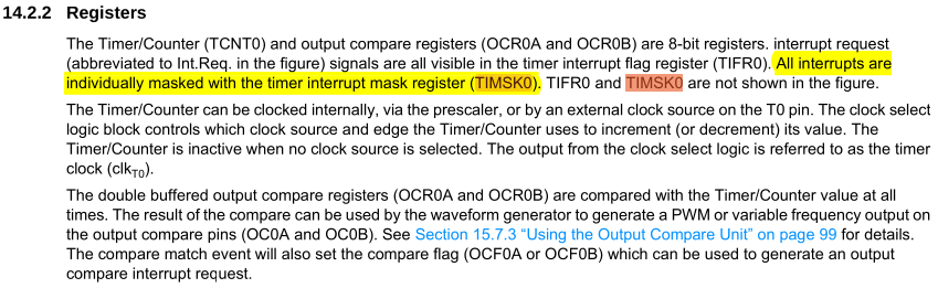
Further expanding, datasheet figures 14-1 through 14-4 unfortunately do not provide much guidance, but TCNT and OCR registers appear to be conditioned by TIMSK as explained in section 14.2.2.
I hadn't considered it until now, but the flag bits in TIFR0 are set when their conditions happen, even if the corresponding TIMSK0 bit is not enabled.
@DaveX just to clarify, the apparent doubling of the prescaler happens only when the entire TIMSK0 line is omitted, i.e. commented altogether.
On the contrary, indeed, setting OCIE0A in TIMSK0 corrects the issue, as shown in the thread opening code sample, without the need of explicitly declaring the corresponding empty ISR. Will definitely bookmark your advise!.
Also, although Atmel didn't explicitly tie the PWM functionality to TIMSK0 in figures nor in register descriptions (as far as I've been able to grasp!), they did 'hint' the possibility of this register playing a role in PWM functionality in 14.2.2:
I don't generally try to decode folks' register configurations, because it's fiddly work that realy ought to be understood and done by the coder using the low-level registers.
I might try this at the end of setup to help confirm that you are setting the registers as planned:
/*
Basic PWM implementation to illustrate the use and handling of timer and comparison registers
*/
void setup() {
// Set pin D6 as output, tied to OC0A register
DDRD |= _BV(DDD6);
// Reset the timer 0 register
TCNT0 = 0;
TCCR0A = 0 ;
TCCR0B = 0;
// Set WGM mode 5: TCCR0A for phase-correct PWM mode with TOP compare at OCR0A
TCCR0A |= _BV(WGM00) | _BV(COM0A0);
// Set TCCR0B for prescaler of 8 and WGM mode 5:
TCCR0B = _BV(WGM02) | _BV(CS01);
// Set OCR0A to 255
OCR0A = 128;
// Enable the Timer/Counter0 Output Compare A Match Interrupt (OCIE0A)
// This is necessary to enable the PWM output on OC0A/PD6
//TIMSK0 |= _BV(OCIE0A);
// Add a small delay to allow the PWM signal to initialize
//delay(100);
Serial.begin(115200);
Serial.println(TCCR0A,BIN);
Serial.println(TCCR0B,BIN);
Serial.println((TCCR0A & 0b11 ) | (((TCCR0B & bit(WGM02)) >> WGM02)<<2));
}
void loop() {
// No need for anything here, as the PWM output is already configured and running
}
//ISR(TIMER0_COMPA_vect){;}
Note the OCR0A = 127 for 50% duty cycle. I'm not sure what Phase correct mode is supposed to do with OCR0A=TOP.
If I set TIMSK0 |= _BV(OCIE0A) without its ISR, I get a 6318Hz, and if I define the ISR, it reverts back to 3907. I think the undefined interrupt re-starts the code, interfering with the cycle.
@DaveX I appreciate your advise although the code is already functional for purpose.
Also, both USART and PWM registers are time-dependent and as such may share timer functionalities that could interfere with each other. As such, I would not advise attempting to troubleshoot PWMs using generic serial communication functions like Serial.println() while also, for instance, going into specific PWM register modification.
And, phase correct when in WGM 5 essentially makes counter TCNT0 start from 0, count up to the value set in OCR0A and then count back down. And, when on 2nd compare output mode COM, it toggles the peripheral digital output once TCNT0=OCR0A or TCNT0=0... effectively clamping the PWM to 50% duty cycle and only allowing to vary the PWM frequency as a function of OCR0A. I hope it makes sense!
Your code in #1 will end up setting WGM mode 7, fastPWM with TOP=255, because the normal initialization is to WGM mode 3, and then setting the WGM02 bit adds 4 to the mode and makes 7.
The PWM registers TCCR0A and TCCR0B aren't time dependent, and you can read what has been written to them and print them to see how they have been configured. If I add a Serial.println(TCCR0A,BIN) line to the #1 code,
#1 code with a couple prints
/*
Basic PWM implementation to illustrate the use and handling of timer and comparison registers
*/
void setup() {
Serial.begin(115200);
Serial.print("\nS");
// Set pin D6 as output, tied to OC0A register
DDRD |= _BV(DDD6);
// Reset the timer 0 register
TCNT0 = 0;
// Set WGM mode 5: TCCR0A for phase-correct PWM mode with TOP compare at OCR0A
TCCR0A |= _BV(WGM00) | _BV(COM0A0);
  // Set TCCR0B for prescaler of 8 and WGM mode 5:
  TCCR0B |= _BV(WGM02) | _BV(CS01);
// Set OCR0A to 255
OCR0A = 255;
// Enable the Timer/Counter0 Output Compare A Match Interrupt (OCIE0A)
// This is necessary to enable the PWM output on OC0A/PD6
TIMSK0 |= _BV(OCIE0A);
// Add a small delay to allow the PWM signal to initialize
//delay(100);
Serial.println(TCCR0A, BIN);
Serial.println('#');
}
void loop() {
static bool printed = false;
if(! printed){
Serial.print("first loop");
printed = true;
}
// No need for anything here, as the PWM output is already configured and running
}