I will expand the matrix in the future. This is a smaller prototype.
ah I see - so the matrix will be 19x19 ultimately.
Yes that is correct.
On my Arduino MEGA (clone) it displays "AJ" each time I short Pin 2 to Pin 22 and "DJ" each time I short Pin 5 to Pin 22.
Perhaps you have a wiring problem.
Do you know if the direction of diodes makes a difference in keypad matrix?
it does
Diodes in keypads are added to deal with "ghosting" meaning preventing keys that are not pressed to appear as pressed.
the schematic you shared would require setting the columns to INPUT_PULLUP mode so you are lucky you made the mistake because the code you use is setting the rows to INPUT_PULLUP mode and the columns to OUTPUT and turning them LOW one at a time and checking what is seen from the row pin.
➜ So that should be fine.
are you missing diodes in the picture?

Hmm I did observe some ghosting happening from time to time. In my setup, diodes were connected to the row wires, but their direction is pointing towards the switch and not the row wire, which is different from most diagram I searched on the internet.
If I were to follow the image completely:

the triagle symbol points away from the switch, which is the side of the diode with the colour stripe, I should set the columns to INPUT_PULLUP mode? If my understanding is correct, I should set the INPUT_PULLUP to be on the side of the source of current permitted by diodes?
p.s. I only constructed the matrix at the lower right corner of the board, so the locations without diodes were still in progress.
I think the 5V thingy at the top of the matrix and the 10kΩ resistors you have in the drawing

do not exist in a real keypad. I suppose they did so to demonstrate the code would put the columns as INPUT_PULUP.
Did you wire those ?
I don't have any resistors in my circuit. My understanding is that the matrix consists of switches, diodes and wires. Anything extra would belong to whatever this matrix is interfacing with. What is INPUT_PULLUP? I looked it up but didn't quite understand the explanation.
so is this how your matrix is wired ?

it's the state of an INPUT pin as if it was wired with an extra resistor and connection to 5V (this happens inside the MCU, and you configure that by software when you call pinMode(pinNb, INPUT_PULLUP);)
So that if you leave the pin floating
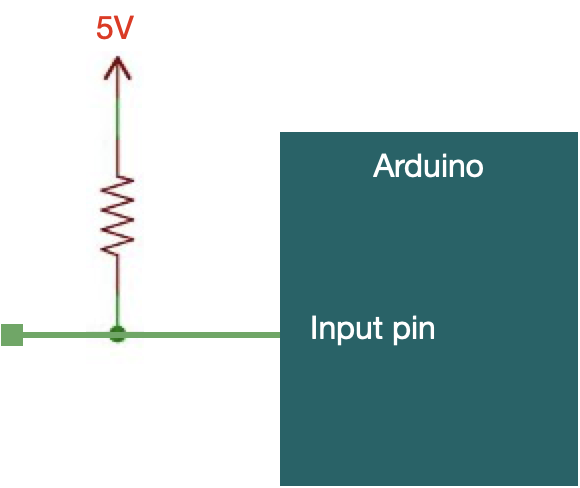
or if you connect it to 5V

then the input pin does see a HIGH
but if you connect it to GND

then the pin does read LOW. (the resistor is there to ensure there is no short circuit).
➜ this is called a pullup as the pin is "pulled up" by default but goes LOW if you connect it to low.
it's very often used with push buttons

Yes the diagram is exactly how my matrix circuit looks like. You are faster at drawing the diagram than me ![]() Thanks a lot for visualizing it! Still reading your response...
Thanks a lot for visualizing it! Still reading your response...
so that should work fine with the way the code is written as it makes the rows INPUT_PULLUP and turns the column to OUTPUT and make them LOW one by one
Does it matter if the input pullup is placed at the row or column? In my diagram the circuit should flow from row to column so does that mean the input pullup should be one the row side?
yes I think so
Hmmm that's odd. I don't think I should see the ghosting I observed. What can I do to triage the issue??
I would start verifying all the soldering and paths
This is what I have built so far. Thank you all for your helps!!

If you post in YouTube and put the YouTube link in the forum everyone will be able to see it without needing to go anywhere to download something
Your matrix should not have pull-ups at all. The library uses the internal pull-up resistors.
I think that's OK as he said
the drawing he used assumes the columns would be made INPUT_PULLUP

but the library does not work that way. I think he got lucky making the mistake
I'm no hardware expert and wonder what potential is read by the pin (at the red dot) in those 2 situations (diode facing towards or opposed to a closed switch connected to ground)

my crude understanding is that in the top case the current from the pullup can flow to GND through the resistor and diode and the pins sees a LOW whereas in the bottom case the diode prevents the current from flowing, so it's like the switch is open and the pin sees a HIGH
➜ that's why I was tempted to say that if the row is made an INPUT_PULLUP and the library pulls to LOW the columns in turn (as in the code of the library does), then the diode must allow the current to go through the switch and so the top drawing is what you want with the library.
happy to be proved wrong though, I'm a software guy...