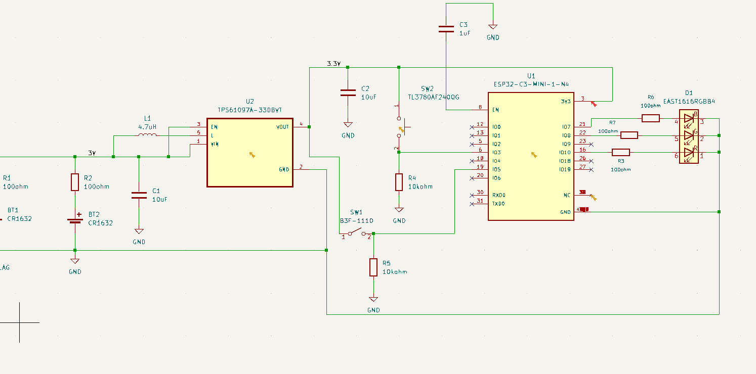
Hey guys! I just want to make sure that the schematic I had made was done so correctly, specifically the button configuration. I want a 10kohm pull-down for each button so I want to make sure that I had routed the buttons to the gpio correctly. Also will the RGB LED have a common anode? On the datasheet for the LED (EAST1616RGBB4 Everlight Electronics Co Ltd | Optoelectronics | DigiKey) the different colors have a common anode such that the LED is only plugged into one gpio. On my current schematic I have it such that each color has its own resistor and gpio, is this allowed?
In short, the circuit works as follows: Pretty much SW1 is to activate the BLE sequence and SW2 is for changing the current state of the board (which will be indicated by the LEDs). Both switches need to wake up the esp from deep sleep so they have to be on gpio0-gpio5. Thanks for the help!
Nice Schematic. How long will the button/switch wires be. If they leave the package I prefer to always switch to ground, that way VCC is not connected to an antenna. Also I like to have switches switch at least one mA so I would switch the 10K to 3.3K resistors. Part of the schematic is missing so I cannot comment on the power supply section.
The power supply is 2 coin cells in parallel (most likely 1632 for maximum mAh due to size constraints). The boost converter will supply a stable 3.3V. The 100ohm resistors decrease the equivalency current between the two parallel batteries.
My question is more geared to the button (if the pull down resistor and gpio connection was done correctly) & the LED (whether each color would have its own resistor and GPIO pin or whether they would be combined in parallel as seen in the datasheet and have 1 GPIO input and 1 resistor)
That would be the best place. I think you would be much happier placing the batteries in series, the resistors will burn a lot of power as heat. That will definitely hurt your run time.
While the circuit around your push buttons will work, I wonder why you havent used the alternate (and generally safer) arrangement of a pull-up resistor (even an internal pull-up) and switch to ground?
That would also allow you to add small capacitors across your switches to do the debouncing.
Batteries can't be in series as that will not increase the current capacity which I need, also the voltage would increase and my boost converter will not work as it is not rated that high
The wattage will remain the same whether in series or parallel. With a buck buck converter the efficiency would be in the 94% + efficiency range. I would also consider using a low side driver such as a MOSFET, very low voltage drop and no load on the port pin of the CPU. The logic would remain the same.
I am realizing now where the confusion is coming from. The schematic in the data sheet on page 2 is a diagram of how your assembly is made. You cannot change it. You can only do as I said in post #6. You have the LED’s drawn in reverse of how they are made.
If you want to light each color individually you can use a separate GPIO for each color. If your ESP cannot sink the required current, you will have to use an external drive transistor for each color . Either way you will have to use a separate ballast resistor calculated using the forward voltage range for each color and the desired current you want to achieve.
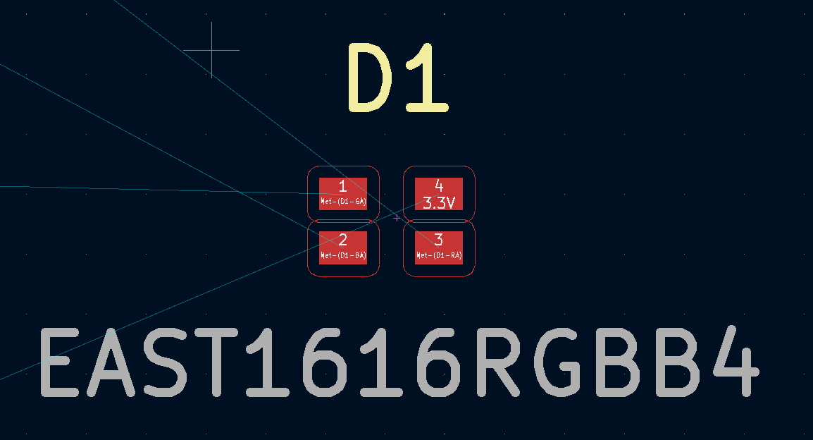
Hi, I just want to check if the LED is implemented correctly this time. Pin 4 is the net for the 3.3V. Pins 1-3 go to a resistor in series which goes to a gpio in the esp32-c3. Thanks for the feedback!
That should work. With the common anode configuration you will have to set the GPIO pin low to turn on the LED’s. The green and blue LED’s also need around 3 volts just to turn them on so your resistor selection will be critical to avoid overloading the I/O pins. Are you going to use PWM to control the intensity of the LED’s?
I was not planning on using PWM or PDM in the current iteration. I am not entirely too familiar with its capabilities. What does PWM allow for me to do with the LED or is it just light intensity?
Also yes, I will test different resistors out on the breadboard using the breakout pcb I designed for the LED (it is way too small to solder jumper wires to each pad). My battery will supply 3V (although the boost converter will step it up to 3.3) and so I was planning on using a 100ohm resistor in series with each of the colors (maybe less for the green since when I tested it, it was dimmer than anticipated).