I've created a new board similar to the Pro Mini - based on the 328P running at 3.3v and 8MHz.
I am using the SparkFun 400mAh LiPo as power. That product include over and under voltage protection, over current protection and shuts off the LiPo at 2.7 v. (Which seems low to me, but I would presume that the manufacturer knows what they are doing.)
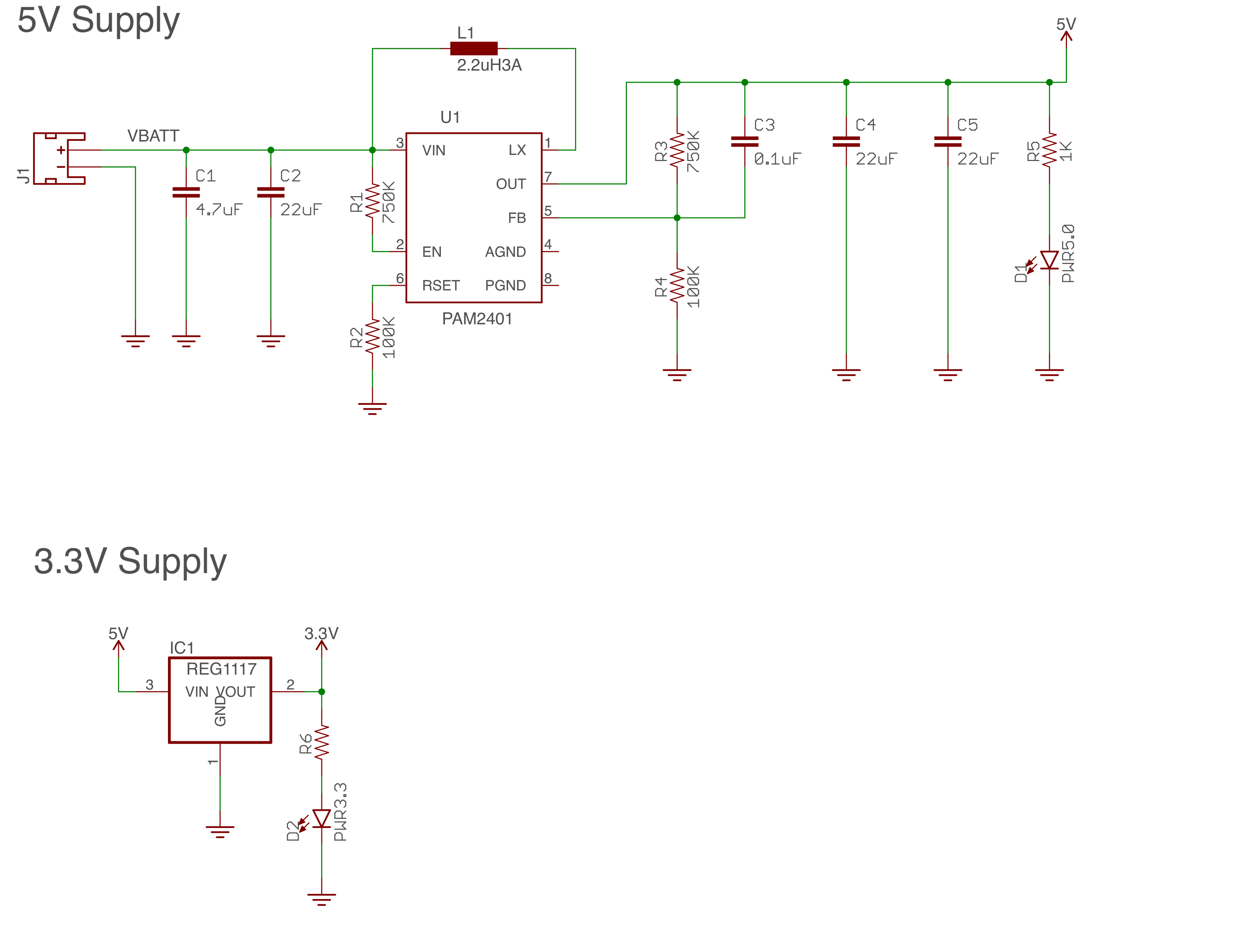
And from the regulated 5v I am using an LM1117IMPX-3.3/NOPB to get my regulated 3.3 for the processor and two other IC's. This device is speced for up to 850mA but I am only using a max of around 100.
I am supporting all of these devices with the components required in their datasheets.
The problem is that the 3.3 regulator jumps to around 2.3 v on initial start up, and then takes a whopping 800ms to ramp up to 3.3v. This is confusing a 3.3v accelerometer to go a bit AWOL.
I suppose I could use an MOSFET for the power rail to the accelerometer and just wait to turn it on after a second or so, but that seems like a bad way to go about it. I'd much rather understand why this is happening and what to do to fix it properly.
Why are AG and PG left open on your schematic? That’s no small error.
The 750K pull-up on EN. Why such a high value?
After working through the above two issues, that leaves the best for last with a switching regulator. What’s the pc board layout look like? It wouldn't be the first time a skinny trace in the wrong place makes a switch mode device throw a hissy fit.
I could conceivably go with only 10uF into the 5v regulator, but the other values are all defined as minimums by the datasheet.
Regarding the AGND and PGND on the PAM2401, I seem to have somehow deleted them when I printed to PDF. They are in fact tied to ground. Corrected schematic attached.
The 750K pullup on EN is just to limit current to a minimum. I guess I could go with, say, 22K but could that be relevant to the problem I am having?
My design rules call for a minimum of 12 mil for all traces, 24 mil for power traces (GND, +5 and +3.3v) and minimum distance between traces of 6 mil. But that said, all of my 3.3 traces have lots of room around them. I will go over the rest of the traces carefully but I'm pretty sure that the only tight ones are on the legs to the ATMega328P.
Is there anything here that I should scope that could be accounting for the long ramp time on 3.3? Or other items I should check?
And, lastly, can anyone recommend a way to design properly around this problem?
A valuable but hard lesson to learn is that there is an extremely high probability that the problem is due to something you did wrong in the implementation. Accept that and work on finding the fault, not “designing around it”.
Start by tying EN high, no resistor. If you’ve still got issues, post your gerbers as pdfs.
As an afterthought, have you monitored battery voltage on power up? Is it stable? Also, do you have a part number/link for the inductor?