Looking for a complete labeled Lilypad diagram

Hi there. I've just started working with an Arduino Lilypad and have done a few simple tutorials.

I'm now trying to connect a BlueSMirf Gold shield to the Lilypad. However, various instructions I've found are lacking details.

For example, this one, by Leah Buechley, is most often referenced, but shows an older version of the Lilypad.

thehighlowtech.com/LilyPad/extend.html

It says nothing about how to power the set up, and (most significant for me) does not say how the pins described map to the hardware.

Theres just a picture of an older board (the current Lilypad, and the BlueSmirf, have six header pins, not four), and this description:

"Attach 5v to PWR, - to GND, tx to RX - I, and rx to TX - O. "

I've found other Web pages describing how to connect things to the Lilypad and they all seem a to assume the reader knows exactly where to find 5v or 3.3v or TX or whatever.

There's nothing on the Lilypad though that indicates what any of the header pins are. So I have no idea what pin is 5v, or tx, etc.

I searched around for this info and have found assorted documents and schematics that may have the info I'm looking for, but it's not in a format I can understand.

The closest thing I found was a Lilypad diagram here:

It's an excerpt from the book Programming Interactivity.

The specific image is

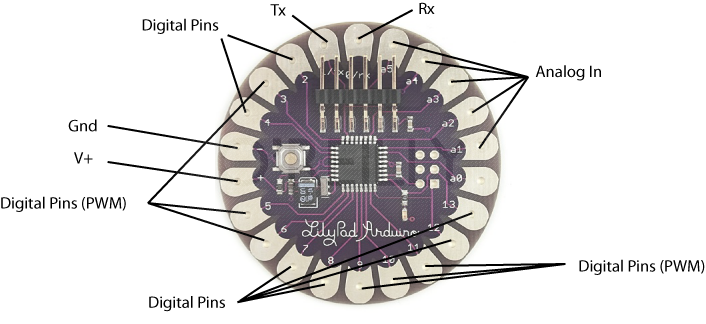
It's almost perfect, but it does not say what the header pins are for (the pins where you would attach a USB link cable).

Does anyone know of such a diagram, something that clearly explains what each and every pin or connector on the Lilypad is for, using a picture or simple drawing of the board itself?

Thanks very much.

There are no labels for the download cable but on the picture you gave the link you can identify what is connected to by reading the labels on the FT232.
For the board on O'Reilly's it is (from top to bottom)
GND
RX
TX
3.3V

If your board has a 6 pins header you can look at the schematic here http://arduino.cc/en/Main/ArduinoBoardLilyPad

Thanks for the reply.

I've looked at the schematics but could not make heads or tails of it.

There is section that looks sort of like this:


|
DTR ----* DTR
TXO ----* RXI
RXI ----* TXO
VCC ----* VCC
GND ----* CTS
GND ----* GND
|

JP2

And late last night I found this:

www.arduino.cc/en/Main/ArduinoBoardPro

It has, I believe, the same header pins as the Lilypad, but labeled.

So I'm thinking that in the schematic the values on the left are the Lilypad pins themselves. I do not know what the values on the right are.

In particular, I see there are two pins labeled GND, but they seem to have different roles.

I -think- this is how things are, based on the image and the schematic:

Starting from 12 o'clock on the LilyPad image, the first pad is Pin 0-RX/D0. Moving counter-clockwise are:

Pin 1 - TX/D1
Pins 2,3,4 - D2, D3, D4
Pin 5 - GND or "-" (ground)
Pin 6 - VCC or "+" (power)
Pins 7,8,9,10,11,12,13,14,15 - D5 thru D13
Pins 16,17,18,19,20,21 - A0 thru A5 (analog pins)

J2, viewing the pins as oriented in the photo, is more tricky - I am basing this pinout on the fact that pin 6 appears to be connected to some SMT part, which I think is a decoupling cap on the schematic (to ground), so pin 1 on J2 would be on the left hand side of that photo:

Pin 1 - DTR
Pin 2 - RX1
Pin 3 - TX0
Pin 4 - VCC
Pin 5 - CTS (pulled LOW to ground)
Pin 6 - GND

Once again, this is all an "educated" guess based on what I can see in the diagram and the photo; take it for what it is worth, which isn't much (if I had one in hand, or a larger photo front and back of the board, it would be easier).

Hope this helps - double check everything I wrote above before using (I really don't trust my guess due to lack of information and not having ever used a LilyPad). Maybe someone else can verify this guess?

:slight_smile:

Thanks for the info. I'm going to see what I can do to verify the details I have; it may involve learning how to read schematics. :slight_smile:

Success!

I'm pretty confident that my pin labeling is correct. After some re-wiring and poking around I was able to:

  • Power the Lilypad by attaching a Lilypad AAA battery pack to the + and - pin tabs on the Lilypad

  • Connect the Lilypad to a Bluesmirf Gold by running connectors from the header pins on the Lilypad (the same opins you would use for the USB connector when uploading a sketch) over to the Bluesmirf. I had to add corresponding pins to the Bluesmirf since it does not have them by default.

The middle 4 pins on the Lilypad went to the middle 4 on the Bluesmirf.

bluesmirf lilypad
green vcc 3.3v
yell gnd gnd
blue tx-o rx-i
red rx-i tx-o

BTW, these just happen to be the wire colors I picked; I have no idea if there is any standard or convention for these things.

(I do stick to using black and red for - and + power though, when hooking up the battery.)

If you rotate the Lilypad so that the header pins are at 9:00 you get this pin assignment (with the wiring colors I happened to pick for connecting to the Bluesmirf):


|
-------- RTS
-------- TX-O red
-------- RX-I blue
-------- 3.3V green
-------- GND yellow
-------- GND
|

I believe that the "top" pin, RTS, is used to doa a reset on the Lilypad when uploading a sketch.

I don't know what that other GND is for.

The upshot is that I could then run the Amarino (http://www.amarino-toolkit.net) Bluetooth app on my G1 phone and pair it with the Bluesmirf running off my Lilypad.

I was having some unreliable behavior, and suspected quirks with the AAA battery hook-up, so I switched that out and connected a 3.3v battery instead, and it worked fine.

If anyone thinks I've gotten something wrong here, please let me know, but it seems about right.

Thanks!


|
DTR ----* DTR
TXO ----* RXI
RXI ----* TXO
VCC ----* VCC
GND ----* CTS
GND ----* GND
|

JP2

Right labeling is FTDI232 download cable pinout

Does this help?

westfw: Yes, thanks, that is fantastic.

And much nicer than my ascii art. :slight_smile:

In the description for the Lilypad 328, it says that six of the I/O pins can do PWM. Does anyone know which ones? I can't find any simple documentation and am admittedly not in the mood to sift through the 420 pages of the ATMEGA's datasheet.

Thanks.

Should be the same as other '328-based models, so PWM on D3, 5, 6, 9, 10, 11.

Jon
Freetronics: www.freetronics.com

Good thinking. It didn't occur to me to look at the other Arduinos using the same uC.

Cheers,

BJ

Added PWM labels: