Smajdalf, one thing I can imagine could cause issues with the low side switching is connecting a programmer. But typically, for this purpose, I disconnect a supercapacitor and connect the programmer.
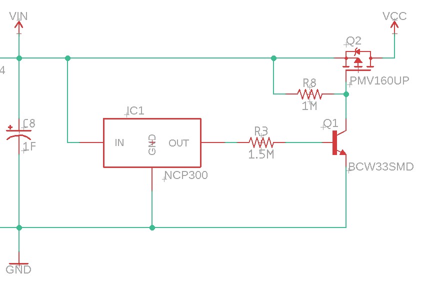
I've played a bit with the previous schematic, really close to this one (but U1 is a different IC, V2 is embedded into U1, R4 is pull-up)
by replacing Q1 with an NFET and increasing pull-up resistors values, I achieved 10uA (3.6V).
But I'll try both schematics, low side switching, in this case, looks too good to ignore (from the power consumption point of view). Probably I'll order two different PCBs to have options.
UPD: raschemmel, haven't noticed your update again
raschemmel:
FYI,In plain English that means that the current the transistor passes is essentially negligible and the only purpose is
serves is to apply 0V to the mosfet gate.
Probably, you should also quote here how BJT transistor works, because we discuss the base resistor for BJT.
As a small current flowing into the base terminal controls a much larger collector current forming the basis of transistor action.
Summarizing: I'll lose power through Base - Emitter of the transistor, and then through R8 and Collector - Emitter of the transistor, and yes MOSFET's gate won't consume almost anything (except during switching), but do you see all other losses here?
UPD2:
Paul__B:
Then use a CMOS logic gate. Not so expensive (and actually, you can get single gates; they come in a 4 or 5 pin SMD).
Seems I've found a nice candidate TPS22917 Ultra-Low Leakage Load Switch. Voltage range: 1V to 5.5V, power consumption 0.5uA.