Before I post the link, I just don't seem to get the principal.
My understanding has always been this, maximum clock speed = processor speed (eg, 5 1ghz does not equal 5ghz) and while
that makes sense, you can share the load between each CPU, eg allocated a CPU to a thread and let it get on with it, kinda like
5 guys taking 1 hour to do the job of 1 man working 5 hours.
But, when it comes to something like an ATMega, we have all kinds of extra things going on.
I've seen this done the RPI too, 16/32 boards all linked to produce a powerful machine... but I still don't get how
controlling 32 of them be 32 Attiny85's, or raspberry pi's or atmega!
Do we have 1 processor which controls every other processor? how's the shifting around of memory work?!
Mind you, they share external RAM and use 8 digital pins to access that RAM, and two control pins. So quite a few of your existing pins are used to get to the RAM (maybe I2C would have been another option).
Also he is using a bytecode (runtime emulation) system so the cores are interpreting bytecode, not running machine code, which would slow them down compared to executing native instructions.
I don't want to "knock" it, it's a great example of how multi-core processors can be made to work together.
Someone had something along similar sorts of lines here a while back: multiple processors stacked together with each one doing it own specialized "thing".
And as he points out, the CPU chips are around $2 each, so you can always get an Atmega328 processor and make it do whatever specialized thing you want, and combine them together for interesting effects.
At the "higher-end" scale of things, this is basically what you are looking for:
The actual individual processing nodes used can be anything from simple 1-bit machines, to complete computers in their own right (beowulf clusters, blades, gpus, etc).
Then you get into the whole networking infrastructure (for memory, data, etc - sharing).
In the microcontroller world, you typically will hang a bunch of "slave" nodes off of some bus (usually SPI), and a master node will dole out the work units to each slave processor, where it will do the work, return the result, then the results will be combined by the master into the final result. The programming to do this isn't very difficult, actually - the difficulty is in finding processes that can be turned into a paralleled algorithm - and also recognizing when a process can't. Certain things are easily identifiable - such as when you are simulating a huge number of interacting but mainly similar particles; or for instance, ray tracing, where segments of a scene can be individually computed (also, fractal algorithms tend to be highly parallelizable).
Basically, if you can vectorize (linear algebra) a serial algorithm, you can optimize it for a parallel processing architecture.
If one ship crosses the ocean in 8 days, 8 ships cannot do it in one day
But sometimes they can 8)
The problem with a big ship crossing is maneuvering out of port, getting up to speed, slowing down again, and maneuvering back into port.
A small boat can do all of that much quicker with much less mass to get up & moving, and with midocean refueling, can keep its mass down & its speed up.
Wikipedia:
The current eastbound record was set by the American ocean liner United States in July 1952: the ship made the crossing in 3 days, 10 hours, 40 minutes.
HSC Sea Runner is a 74 m (243 ft) ocean-going catamaran built in 1990 by International Catamarans (Incat) for the UK company, Hoverspeed. In 1990, she took the Hales Trophy for the fastest eastbound transatlantic journey, making the run, without passengers, in three days, seven hours and fifty-four minutes, averaging 36.6 knots (67.8 km/h).
Down at the bottom of this link
New York[20] 1823-4 16 Dec-1 Jan Black Ball Line New York Liverpool 3,248 nautical miles (6,015 km) 15 d 16h 8.63 knots (15.98 km/h) (376 hours)
vs
Cat-Link V (or today Fjord Cat) 1998 20 July Fjord Line 2 d, 20 h, 9 m 41.3 knots (76.5 km/h) (68 hours)
So, still not quite 1/8 the time, but a pretty impressive improvement (over a 174 year time span).
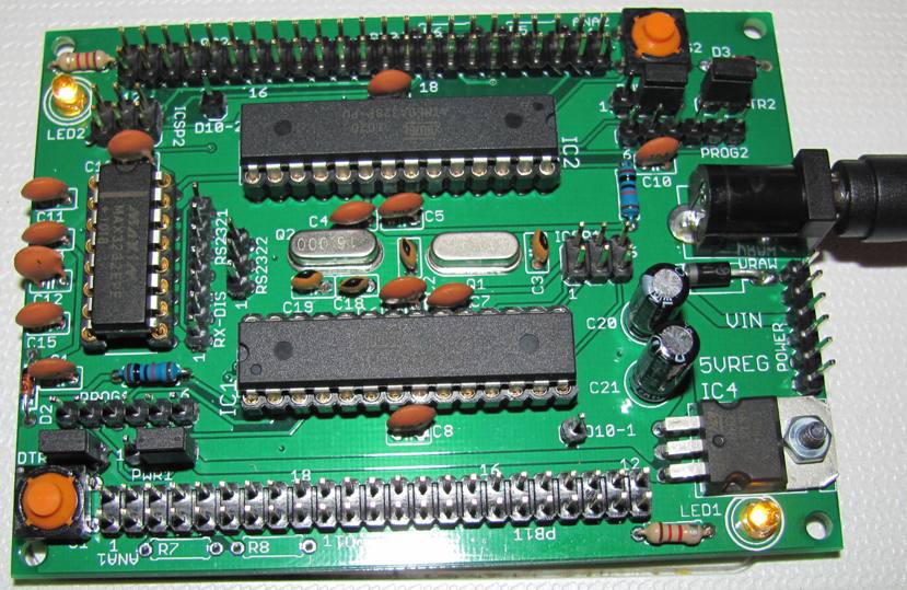
I did a dual processor device last week. I wanted to run a 240-LED WS2811 strip alongside some other stuff which had fairly hard real time constraints (NRF24L01 radio receiver and an ultrasonic distance sensor which needed interrupts enabled).
Updating 240 LEDs takes about 8ms so it broke the real-time constraints. I added a Tiny85 to handle the LEDs and free up the main CPU (an Arduino Uno).
I made a dual '328 board. No time to write a really interesting program to share data or something between the two tho to put it thru its paces.
Can connect each via I2C, SPI, Serial, other pins, jumpers allow RS232 if desired also. Bootload both parts as Unos, plug in USB/Serial adapter modules for serial downloads, or just program via ICSP. http://www.crossroadsfencing.com/BobuinoRev17/
CrossRoads:
I made a dual '328 board. No time to write a really interesting program to share data or something between the two tho to put it thru its paces.
The overhead for communications would probably negate the extra CPU power.
It hardly seems worth using multiple AVR chips for extra computing power when a single ARM chip would be equal to dozens of them and have far more RAM (and be much easier to program). The place I think it makes most sense to use multiple AVRs is as slave chips for things where timing/response is critical.
The concept of multiple microcontrollers in a system is very common. I design them all the time - one master controller MCU with a number of slave MCUs to do specific jobs, such as human interfaces (buttons, switches, knobs, displays etc), sensor interfacing and data normalizing, etc.
Even your lowly Arduino UNO is a multi-MCU system. You have the ATMega328P as the "master" MCU, and an ATMega8U2 as a slave MCU for dealing with the USB interfacing. The USB interface is pre-programmed to do a specific task and just communicates with the "master" MCU through a well-known protocol.
Done right you don't even really think of the slave MCUs as MCUs at all, but as chips that just do a certain job. Once their firmware is written (and working right) they can be almost forgotten about and just used as any other component.
I'm in the process of debugging such a system right now. It has three atmega cores that are "co masters", communicating through shared external RAM.
Seemed like the easiest way to approach parallel real-time processes like wireless, encoder or sensor monitoring, etc.
infact, he's using 1 processor per scan line, how about 1 processor for 4 pixels, 2pixels even 1 pixel?... attiny85's right down to the smallest size processor on the nano scale, and then mount them all on 1 stamp sized cpu, have the wires bonded inside 1 "cpu" - having a credit card sized 8bit mega computer, on the credit card, we have a small 5v solar panel with a regulator to supply to the power to this monster.... with data retrieval is a form of NFC, to communicate, you then talk to the main processor which has the ability to flash any of the chips with the new arduino firmware...
800 x 600
= 480000 pixels / 8 bit processors
that a FEW too many cores?? - but with that system you could allocate 1 pixel and bring a computer to life.... right?
cjdelphi:
you can share the load between each CPU, eg allocated a CPU to a thread and let it get on with it, kinda like
5 guys taking 1 hour to do the job of 1 man working 5 hours.
It all depends on the job. You can't make a baby in one month by putting 9 women to work on it.
cjdelphi:
you can share the load between each CPU, eg allocated a CPU to a thread and let it get on with it, kinda like
5 guys taking 1 hour to do the job of 1 man working 5 hours.
It all depends on the job. You can't make a baby in one month by putting 9 women to work on it.
No, but it can make you wish you hadn't started trying 9 times faster
Oh., and make sure they never find out about each other, or all chance of ever having offspring will be somewhat curtailed...