I have bought the 4051 multiplexer for my arduino project. I want to read from multiple analog inputs (coming from piezo discs), but am having trouble wading through the process of understanding the code, as I am mostly a virgin when it comes to programming. I'd like to have the multiplexer cycling through all 8 pins constantly, while prepending an alphabetical letter to each reading in order to identify which pin it came from.
void loop () {

  for (count=0; count<=7; count++) {

    // select the bit
    r0 = bitRead(count,0);    // use this with arduino 0013 (and newer versions)
    r1 = bitRead(count,1);    // use this with arduino 0013 (and newer versions)
    r2 = bitRead(count,2);    // use this with arduino 0013 (and newer versions)

    //r0 = count & 0x01;      // old version of setting the bits
    //r1 = (count>>1) & 0x01;      // old version of setting the bits
    //r2 = (count>>2) & 0x01;      // old version of setting the bits

    digitalWrite(2, r0);
    digitalWrite(3, r1);
    digitalWrite(4, r2);
I am at a loss trying to understand what this part of the code is trying to achieve. I've looked up the terms but in connection to the multiplexers function, I am struggling to understand. Can anyone help me rework the code to perform the operation I mentioned above?
When you ask a question that involves the function/behavior/use of an ic it is customary to upload the datasheet as a courtesy to
minimize the time spent by those who respond. Failure to upload the datasheet can and does discourage people from responding to your question because they may assume (correctly or incorrectly ) that you are lazy and trying to dump all the work on them.
We try not jump to conclusions so could you please post the datasheet for the 4051 you are using ?
I was under the impression that 4051 multiplexers were all the same, and that the link I supplied would be enough. No datasheet came with the component in shipping. I thought of it as a passive switch component and wasn't aware more information was needed.
I was under the impression that 4051 multiplexers were all the same, and that the link I supplied would be enough. No datasheet came with the component in shipping. I thought of it as a passive switch component and wasn't aware more information was needed.
Ok, let's go through this step by step so you don't miss anything. Let's look at the facts we have. FACT #1 : You are currently using or plan to use an HEF4051, 74HC_HCT4051, or a CD4051. FACT #2: You are using a tutorial, (see attached sketch) FACT #3: You are perplexed by some code you found in the tutorial
I am at a loss trying to understand what this part of the code is trying to achieve. I've looked up the terms but in connection to the multiplexers function, I am struggling to understand. Can anyone help me rework the code to perform the operation I mentioned above?
THIS CODE:
FACT #4:
You DID NOT READ THE DATASHEET BEFORE DOING THE TUTORIAL:
I was under the impression that 4051 multiplexers were all the same, and that the link I supplied would be enough. No datasheet came with the component in shipping. I thought of it as a passive switch component and wasn't aware more information was needed.
Ok, now that we have all the facts, lets look at the question again and see if we can find any reason why you should read the datasheet.
First statement :
So we can see from this tutorial on FOR LOOPS that this program is sequencing LEDs and needs to count from 1 to 8 to do that :
for (int thisPin = 2; thisPin < 8; thisPin++) {
Well, that looks remarkably similar to this:
for (count=0; count<=7; count++) (from our code)
So we can conclude that statement is a loop count ing from 0 to 7 , which is like counting from 1 to 8. Why EIGHT ? Why would this program be counting from 1 to 8 instead of any other combination of numbers ? Well, let's cheat and look at the datasheet (don't tell ANYONE YOU DID THAT)
The HEF4051B-Q100 is an 8-channel analog multiplexer/demultiplexer
Ah hah! That's why! It has to select all 8 channels one at a time. There you go . Case closed.
Next line:
 // select the bit
    r0 = bitRead(count,0);    // use this with arduino 0013 (and newer versions)
    r1 = bitRead(count,1);    // use this with arduino 0013 (and newer versions)
    r2 = bitRead(count,2);    // use this with arduino 0013 (and newer versions)
bitRead ? Let's see what we can find about that .
bitRead()
Description
Reads a bit of a number.
Syntax
bitRead(x, n)
Parameters
x: the number from which to read
n: which bit to read, starting at 0 for the least-significant (rightmost) bit Returns
the value of the bit (0 or 1).
Well if we look at our code;
x=count
n=2,1,0
This seems to be important:
n: which bit to read, starting at 0 for the least-significant (rightmost) bit
If the multiplexer needs an address that changes incrementally by 1, then what it needs is three pins than count in binary
like a microprocessor or a software function , like bitRead.
But how do you count in binary ?
Ok, so if this code is counting in binary using r0 ,r1 , & r2 , then the address on the multiplexer is changing but why ? The code
we have been given is not reading or writing any analog values to or from the multiplexer. So what is going on here ?
Let's go back to the tutorial" http://playground.arduino.cc/learning/4051#.UzN8RPldW_j
What does it say here ? (the two lines down from the digitalWrite statements) //Either read or write the multiplexed pin here
What ? The OP left out the most important line in the whole tutorial code !
All that code is just to increment the address lines and the user is supposed to INSERT their analog read or write statements
right after the line that says: //Either read or write the multiplexed pin here
I think it's time we took a closer look at the datasheet:
What's this ?
VCC and GND are the supply voltage pins for the digital control inputs (S0 to S2, and E).
The VCC to GND ranges are 2.0 V to 10.0 V for 74HC4051
and 4.5 V to 5.5 V for 74HCT4051
But I thought all 4051's were the same !
I was under the impression that 4051 multiplexers were all the same,
So bottom line, if you are using the 74HC4051, you can connect 2 to 10Vdc to Vcc & grnd
if you are using the 74HCT4051 your Vcc must be 5Vdc.
What is Vee?
The analog inputs/outputs (Y0 to Y7, and Z) can swing between VCC as a positive limit and VEE as a negative limit.
VCC - VEE may not exceed 10.0 V.
For operation as a digital multiplexer/demultiplexer, VEE is connected to GND (typically ground).
Ok. Well I guess that explains that, now what about this code ?
Next group:
  //r0 = count & 0x01;      // old version of setting the bits
    //r1 = (count>>1) & 0x01;      // old version of setting the bits
    //r2 = (count>>2) & 0x01;      // old version of setting the bits
What is this ">>" ?
Evidently , that was the old way to count in binary.
More old stuff. We'll come back to this later to see why it was here.
Last group:
This is the code we need to focus on because this is what we are running.
Let's look at the definitions in the tutorial:
int r0 = 0; //value of select pin at the 4051 (s0)
int r1 = 0; //value of select pin at the 4051 (s1)
int r2 = 0; //value of select pin at the 4051 (s2)
Huh, look at that. It seems to be referring to some so-called "Select Pins for the 4051" (time to look at the datasheet again....)
The HEF4051B-Q100 is an 8-channel analog multiplexer/demultiplexer with three address
inputs (S1 to S3)
What , it's supposed to say S0 to S2 ! What's going on here ?! OOPS! WRONG DATASHEET ! Darn ! I thought all 4051's were the same ! Wait,that sounds familiar. Where have I heard that statement before ? Oh, I remember !
It was here :
I was under the impression that 4051 multiplexers were all the same, and that the link I supplied would be enough. No datasheet came with the component in shipping. I thought of it as a passive switch component and wasn't aware more information was needed.
Better check the other datasheet:
CD4051BM/CD4051BC is a single 8-channel multiplexer
having three binary control inputs. A, B, and C
WHAT ! Now we are using LETTERS ?! WTF ! That's it . I've had it. I'm going to check the last datasheet:
The 74HC4051; 74HCT4051 is an 8-channel analog multiplexer/demultiplexer with three
digital select inputs (S0 to S2)
BINGO ! Now we're cookin' with gas.....
Ok , so there it is. the S0, S1 &S2 pins of the 74HC4051 are the Select pins . But wait, what did they call those in the other datasheet ?
The HEF4051B-Q100 is an 8-channel analog multiplexer/demultiplexer with three address
inputs
ADDRESS PINS ! THAT'S IT ! These are the pins that take a binary-weighted address (1,2,4).
Well I guess that's it then. Let's go back and re-read the OP's question to see if we answered it :
as I am mostly a virgin when it comes to programming. I'd like to have the multiplexer cycling through all 8 pins constantly, while prepending an alphabetical letter to each reading in order to identify which pin it came from.
Well I see a problem with that already.
while prepending an alphabetical letter to each reading in order to identify which pin it came from.
I'd like to have the multiplexer cycling through all 8 pins constantly,
We are talking about an ANALOG multiplexer. An alphabetical letter is a an ASCII byte data type. Not only is it DIGITAL and not ANALOG , it is more that one bit, it is eight bits which comprise a byte. Yeah, that's not going to happen pyrocist. That's APPLES & ORANGES. (ANALOG & DIGITAL).
You can't mix analog and digital signals together but there are ways to do what you want.
I have been know to write extensive answers whilst taking a break (usually associated with having to travel for tertiary referral medical tests or procedures like last week), but that one takes the cake!
When you stop laughing can you tell the OP how to use a CASE statement (or IF statement) do trigger an alphabetical letter
(A,B, C etc..) output (serial or lcd) using the multiplexer address line variables r0, r1,r2 ? His question was how to append the alphabetical letter to the analog signal... (don't ask).
That was quite the reply! Its really encouraging to see how much length people are willing to go to to introduce newcomers
I hope you don't think I'm lazy/stupid or anything because I didn't know about datasheets. I know very little about circuitry, so I just... well, didn't know what they were or that they existed tbh, and therefore didn't know I was missing information that should have been supplied! Just wanted to point that out cuz I don't want to come off as a boy that expects everything handed to him on a silver platter. I did also do my research on the code terms, components, and circuitry terms. Sometimes having the same thing explained to you in a different way can communicate better, and I think you achieved that! While I already grasped the functionality and ins-outs of the de/multiplexers etc, your dissection of the bitread code section lead me to the eureaka moment, so immense thank yous!!
I wanted to prepend a letter to the end of the readings because I wanted to send them to Max/MSP (graphic surface coding environment for MIDI/A/V), where the readings could then be routed by their prepended letters in such a way that pin y0-y7 would all be treated differently and appropriately. I found out how now. Below is my roundabout way of writing the code before reading your replies, with the alphabetical addition at the end!
const int ledPin = 13; // led connected to digital pin 13
const int threshold = 50; // threshold value to decide when the detected sound is a knock or not (N/A for now)
const int zpin = A0; // the multiple piezo voltages is sent to analog pin 0
int sensorReading = 0; // variable to store the value read from the sensor pin
int ledState = LOW;
int r0 = 0; //value of select pin at the 4051 (s0)
int r1 = 0; //value of select pin at the 4051 (s1)
int r2 = 0; //value of select pin at the 4051 (s2)
int count = 0; //which y pin we are selecting
void setup(){
pinMode(2, OUTPUT); // s0
pinMode(3, OUTPUT); // s1
pinMode(4, OUTPUT); // s2
pinMode(ledPin, OUTPUT); // declare the ledPin as as OUTPUT
Serial.begin(9600); // use the serial port
}
void loop () {
//FOLLOWING ACTIVATES y5
digitalWrite(2, LOW);
digitalWrite(3, LOW);
digitalWrite(4, LOW);
//Either read or write the multiplexed pin here
// read the sensor and store it in the variable sensorReading:
sensorReading = analogRead(zpin);
Serial.print("A");
Serial.println(sensorReading);
delay(250); // delay to avoid overloading the serial port buffer
digitalWrite(2, HIGH);
digitalWrite(3, LOW);
digitalWrite(4, LOW);
//Either read or write the multiplexed pin here
// read the sensor and store it in the variable sensorReading:
sensorReading = analogRead(zpin);
Serial.print("B");
Serial.println(sensorReading);
delay(250); // delay to avoid overloading the serial port buffer
digitalWrite(2, LOW);
digitalWrite(3, HIGH);
digitalWrite(4, LOW);
//Either read or write the multiplexed pin here
// read the sensor and store it in the variable sensorReading:
sensorReading = analogRead(zpin);
Serial.print("C");
Serial.println(sensorReading);
delay(250); // delay to avoid overloading the serial port buffer
digitalWrite(2, HIGH);
digitalWrite(3, HIGH);
digitalWrite(4, LOW);
//Either read or write the multiplexed pin here
// read the sensor and store it in the variable sensorReading:
sensorReading = analogRead(zpin);
Serial.print("D");
Serial.println(sensorReading);
delay(250); // delay to avoid overloading the serial port buffer
digitalWrite(2, LOW);
digitalWrite(3, LOW);
digitalWrite(4, HIGH);
//Either read or write the multiplexed pin here
// read the sensor and store it in the variable sensorReading:
sensorReading = analogRead(zpin);
Serial.print("E");
Serial.println(sensorReading);
delay(250); // delay to avoid overloading the serial port buffer
digitalWrite(2, HIGH);
digitalWrite(3, LOW);
digitalWrite(4, HIGH);
//Either read or write the multiplexed pin here
// read the sensor and store it in the variable sensorReading:
sensorReading = analogRead(zpin);
Serial.print("F");
Serial.println(sensorReading);
delay(250); // delay to avoid overloading the serial port buffer
digitalWrite(2, LOW);
digitalWrite(3, HIGH);
digitalWrite(4, HIGH);
//Either read or write the multiplexed pin here
// read the sensor and store it in the variable sensorReading:
sensorReading = analogRead(zpin);
Serial.print("G");
Serial.println(sensorReading);
delay(250); // delay to avoid overloading the serial port buffer
digitalWrite(2, HIGH);
digitalWrite(3, HIGH);
digitalWrite(4, HIGH);
//Either read or write the multiplexed pin here
// read the sensor and store it in the variable sensorReading:
sensorReading = analogRead(zpin);
Serial.print("y5 ");
Serial.println(sensorReading);
delay(250); // delay to avoid overloading the serial port buffer
}
Obviously I'll replace delay(250) with a lower variable for faster cyclical readings when the time comes.
Thanks again! Code concepts are clear now. Application starts tomorrow morning
Ok, so I have the code working now. I've adapted it to read just one pin for the moment (y0). However, it seems that I am somehow still able to read every pin at once, which is obviously not possible right?!! I think my piezos are sending out too think a voltage, so I thought I'd use the 5V out from the arduino instead.
If I apply 5V to each input pin, I get a high reading for each one, even though I haven't changed what the address lines of the S0,S1 or S2 inputs.
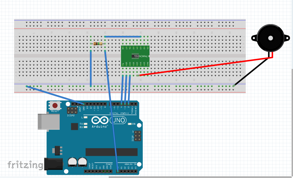
It is the CD4051BE multiplexer. I've attached the datasheet, my arduino code, and my layout. Can anyone spot what the problem is? Hope I'm not being really thick now. I'm wondering if the components are just cheap and ineffective...
Ok. Let's review what we know so far. You some code that count from 0 to 8 in binary and the variables that represent bits 0,1,& 2
are used to control the address lines of the multiplexer. For the benefit of the readers who haven't noticed you chopped off part of the code in your initial post, let's show them what you started with:
/*
* codeexample for useing a 4051 * analog multiplexer / demultiplexer
* by david c. and tomek n.* for k3 / malm� h�gskola
*
* edited by Ross R.
*/
int r0 = 0; //value of select pin at the 4051 (s0)
int r1 = 0; //value of select pin at the 4051 (s1)
int r2 = 0; //value of select pin at the 4051 (s2)
int count = 0; //which y pin we are selecting
void setup(){
pinMode(2, OUTPUT); // s0
pinMode(3, OUTPUT); // s1
pinMode(4, OUTPUT); // s2
}
void loop ()
{
for (count=0; count<=7; count++)
{
// select the bit
r0 = bitRead(count,0); // use this with arduino 0013 (and newer versions)
r1 = bitRead(count,1); // use this with arduino 0013 (and newer versions)
r2 = bitRead(count,2); // use this with arduino 0013 (and newer versions)
//r0 = count & 0x01; // old version of setting the bits
//r1 = (count>>1) & 0x01; // old version of setting the bits
//r2 = (count>>2) & 0x01; // old version of setting the bits
 digitalWrite(2, r0);
            digitalWrite(3, r1);
            digitalWrite(4, r2);
//Either read or write the multiplexed pin here
}
}
This is the part that drives the address lines:
for (count=0; count<=7; count++)
 {
    // select the bit
    r0 = bitRead(count,0);    // use this with arduino 0013 (and newer versions)
    r1 = bitRead(count,1);    // use this with arduino 0013 (and newer versions)
    r2 = bitRead(count,2);    // use this with arduino 0013 (and newer versions)

    digitalWrite(2, r0);
    digitalWrite(3, r1);
    digitalWrite(4, r2);
    //Either read or write the multiplexed pin here
  }
And then you removed ALL of the addressing code leaving only this: (more or less)
  //FOLLOWING ACTIVATES y5

    digitalWrite(2, LOW);
    digitalWrite(3, LOW);
    digitalWrite(4, LOW);

    //Either read or write the multiplexed pin here

    // read the sensor and store it in the variable sensorReading:
    sensorReading = analogRead(zpin);
    Serial.print("A");
    Serial.println(sensorReading);
      // delay to avoid overloading the serial port buffer
So now you are simply setting the address lines to the binary address B000, and reading the sensor. (based on code posted in your last post.)
Ok, so I have the code working now. I've adapted it to read just one pin for the moment (y0). However, it seems that I am somehow still able to read every pin at once, which is obviously not possible right?!! I think my piezos are sending out too think a voltage, so I thought I'd use the 5V out from the arduino instead.
I don't know what you think you are doing here but if you want to test the multiplexer input you need to ground inputs 1-7 while applying 5V to input 0. Then change it to ground all but input 1 to which you apply 5V. Since you removed the addressing code that increments the address lines you will not be able to measure anything on inputs 1-7 because you are selecting line 0 with
all the address lines LOW.
I have no idea what this means :
I think my piezos are sending out too think a voltage, so I thought I'd use the 5V out from the arduino instead.
This is driving me craaaaazy!
Can you elaborate ? What seems to be the problem ?