TEM CAPABILITY
Material FR-4 0.6mm-2.0mm 1oz copper ('standard' PCB material is 1.6mm thick, but we default to 1.2mm)
Layer number 2L
Maximum size 600600mm (6060cm)
Shape Almost anything! We'll send it and see if they accept it!
Min internal slot 32mil (0.8mm)
Min core thickness 4mil 0.08mm
Min core thickness 16-96mil(inner) 16-118mil(out)
Min w/s 6/6mil(I/L) (increased from 5/5 due to poor yield)
Min w/s 6/6mil(O/L) (increased from 5/5 due to poor yield)
Min silkscreen line 0.15mm
Min BGA size Oblong:1013.5mil/circle:12mil
Min SMD width 8mil
Min solder dam 3mil(green)/3.5mil(black)
Min dielectric thickness 2.5mil
Min diameter of finished hole 12mil
Tolerance of drill position +/- 2mil
Tolerance of finished hole size PTH +/- 3mil
Tolerance of finished hole size NPTH: +/- 2mil
PTH hole copper thickness 0.6~1.4mil
Max A.R of PTH 8:1
Surface copper thickness 1oz
Routing dimension tolerance (Z0) Impedance control 4mil
V-cut/V-groove 80mm (8cm) minimum, 380mm maximum. Optional, extra charge
(Z0) Impedance control +/- 15%
Ionic contamination < 6.4ugNaCl/inch2
Surface treating HASL (hot air surface leveling, not PB free unless special request)/AuSn/AgCN/Electrogilding/Ni/OSP/G.F
*OSP Organic solder-ability Preservatives
For best results don't torture the board house! Be conservative. After all, these are crappy PCBs!
As far as I can tell,
"Please note: only one separate design is allowed in each order. Panelized designs are OK for 2 layer boards only, but the boards must be connected by tabs (mouse bites and slots) that snap apart later! Separate, non-connected boards will be refused by the board house!"
Means my board is fine as it is the same design and not separate designs on one board?
I have printed the board on to paper and the bits seem to "fit"...I am more concerned about like hole sizes...tracks...and...stuff?
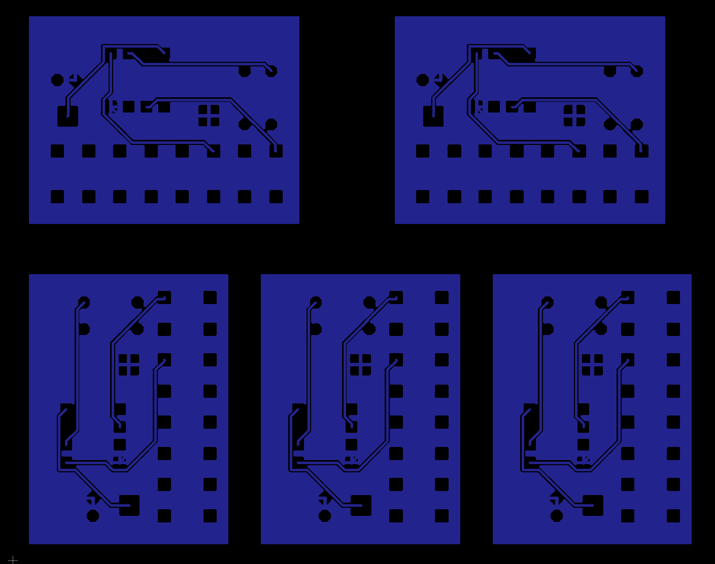
Just about all of your tracks are sliding right up against other "stuff". You should give yourself more space. Sure, the board house says they can handle those tolerances but why test them?
Adjust your default grid to .025" or even smaller and you'll have an easier time getting tracks set right.
You need at least one .1uF capacitor between GND and VCC on any IC on any board, and then it never hurts to go overboard with extra capacitors if you have the space - nobody will force you to populate them, but if you find out you need them when you're putting your circuit together you'll be happy to have those spots available. De-coupling.
Typical rule for polygons is that the top polygon is VCC and the bottom is GND. Somehow your bottom plane is "GND4" which makes me wonder how many voltages you expected to deal with.
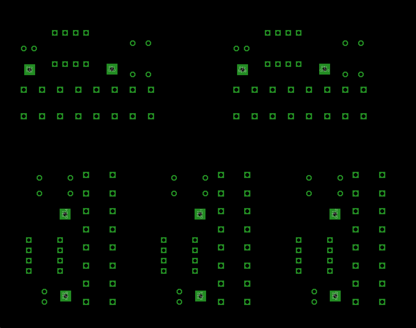
Personally I like to create mounting holes in the corners of all my boards (you can do this with a big via).
You didn't include your schematic; I'm too lazy to check for any problems there.
Eagle will automatically isolate any vias you add in. That should be apparent after you add the via and click the "ratsnest" button.
Also, you might want to try out that "Layer Settings..." button and deselect "tstop" and "bstop". It's only a visual thing; unchecking those makes it a bit easier to see what's going on.
Hi,
I have highlighted a couple of rerouting of tracks to help clearances.
I would be making my tracks thicker.
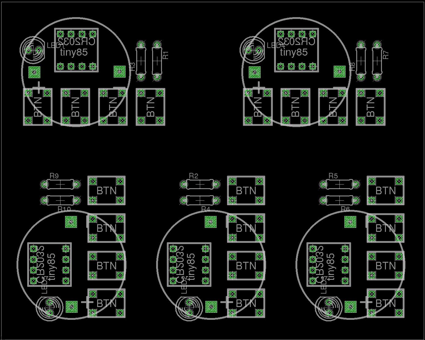
Make you solder pads for the buttons bigger as they have to be mechanically sound as well as electrically.
You have lots of copper to use as conductive tracks, use it for conducting your circuit.
I have re-done the packages a little (bigger pads and labelling more clearly).
I have made the traces at 14mil and manually routed to try keep as much distance as possible.
I have added a small cap for smoothing across VCC-GND.
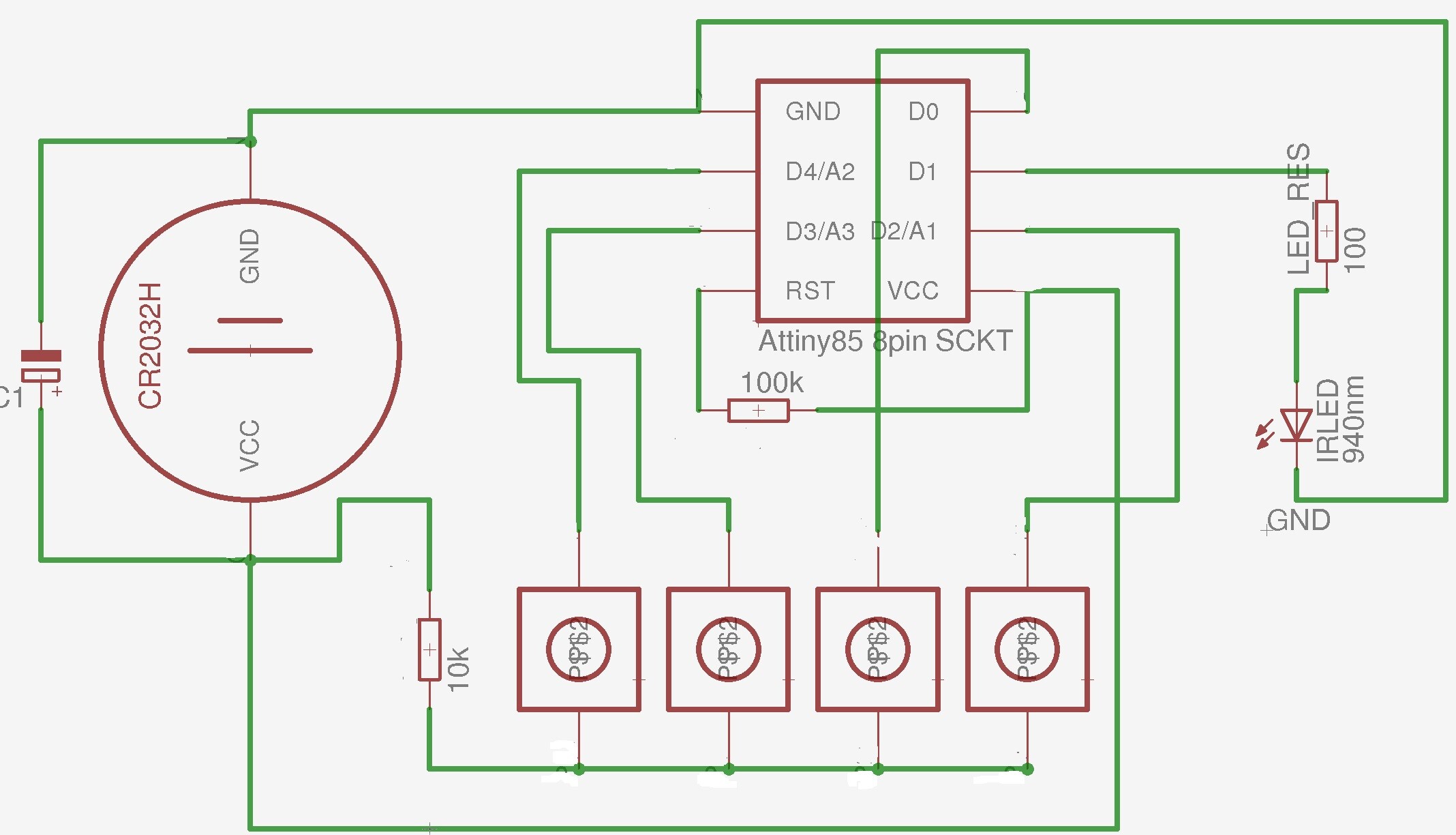
I am using a current limiting resistor from VCC of 10k ohm though the buttons to the GPIO pins of the attiny85.
PB1 (Pin Digital 1) is reserved for my PWM signal for the LED, through a 100 ohm resistor, a 940nm IR LED and to GND.
The battery is a CR2032 (3.6V charged).
I have used a 100k ohm resistor to keep RST pin of attiny85 HIGH. It seems like floating it is fine on the breadboard circuit...but I should keep it right?
Hi,
The re-edit looks good, but, the schematic looks half finished, just having labels on component leads instead of lines representing the wiring does not make your diagram very readable.
I have seen this done in so may places with more complicated circuits and it doubles the time to trace signal flow.
Please can you place wires between your components?
OPs circuit close up.
Thanks.. Tom..
PS. Its not your fault but what cheeses me off about Eagle is all the un-necessary faded text and different washed out colours it uses in its schematics, whats wrong with Black on White?
I have made more clearance between bits...and increased the "isolate" value between the GND/VCC planes and the routes to 0.024" (24mil). The Routes are all ~0.05" (50mil).
I have added 4 Vias as mounting holes, with M1.6 hole size (0.06299213"...about 63mil = ~1.6mm)
You just need to identify pin 1 of the Attiny85, I notice you have used the Attiny85 Socket as a component, is there an Attiny85 in the library as a component. The socket does not show the orientation of the chip, that is pin 1.
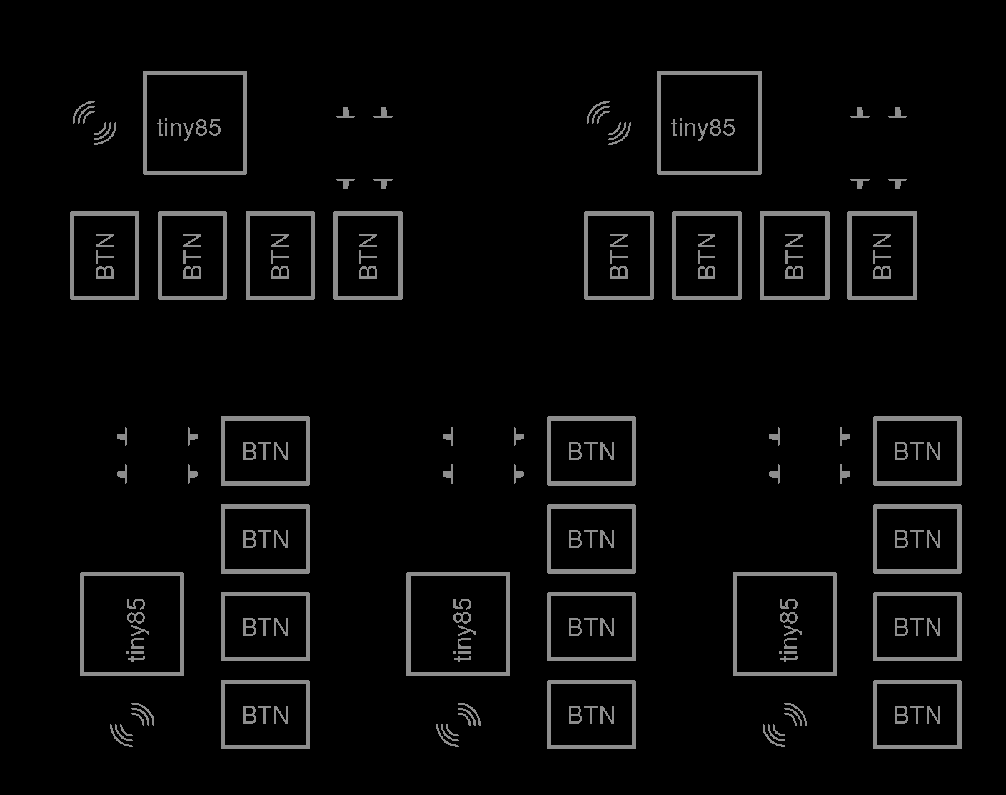
The press buttons need to be shown as switches, not as their PCB image.
Its not you fault but is there a way to get rid of all the doubling up of text?
Somewhere in parameters there must be some to switch off.
I have rubbed out some text to show how much cleaner Eagle can be if they miniimised their default params to display the basic simple schematic.
Used the DirtyPCBs provided files to do the DRU check thingy and the CAM file GERBER outputs...so yeah. Hopefully going to re-check this before tomorrow and then get it sent off!
Can I suggest on your silkscreen overlay print a PCB name and say V1.0 so you can identify it.
Also put a number 1 next to pin 1 of the socket as well so you can see it with the socket fitted.
So you mistakenly don't fit the IC the wrong way round.
Used the DirtyPCBs provided files to do the DRU check thingy and the CAM file GERBER outputs...so yeah. Hopefully going to re-check this before tomorrow and then get it sent off!
Mounting Holes? I see you have some thru holes in the corners, but what are their diameters?
a small #4 screw needs 3.5mm dia hole, and a 7mm diameter pad (0.138" Hole, .276" Pad)
With your Ground and Vcc layers, I suspect you would not be able to use your mounting holes without shorting out VCC to Gnd.
When I use #4 screws, I leave a 10mm clearance (keepout) to minimize the potential for shorting out any signals.
Per DirtyPCB's faq, "separate unconnected designs will be refused by the board house".
If you want multiple board designs to count as one design, you must panelize it your self - in this case, that means drawing the boundary between them on the milling layer, complete with the "rat bites"
I will take this in to consideration next time! I hadn't really considered the mounting very well. Was hoping I can borrow a laser cutter where I work to have basic perspex casing...but I am tempted just to have these on keyring and not really bother with a casing as such.


