Why they are using 100k with Subsystem1, 2, 3 which are connected to P1, P4, P5 respectively and no resistor with Controlled Device which is connected to P3 ? And why 100k specifically ? isn't it too much ?
Decopling caps are recommended for each chip to filter digital noise from the power supply. 0.1uF across the power to the chip as close to the chip as possible.
They use high value resistors for pullup. Each PCF8574 GPIO output can only source* up to 300uA so, I suppose, the pullups need to be high resistance. Since we don't know what those subsystems consist of there is no telling why they need pullups. I don't know what the switch at the bottom is doing.
What do you need the I2C expander for? The MCP23008 8 bit I2C expander will source or sink 25mA from each GPIO output, has internal pullups that can be enabled and has pin change interrupts. May be a better solution.
*IOL LOW-level output current VOL = 1 V; VDD = 5 V Iol(max) = 25 mA sink
IOH HIGH-level output current VOH = VSS Ioh(max) = 300 uA source
There are symbols on the diagram that appear to indicate those are being used as inputs, while P0 uses a similar symbol indicating output. P2 and P3 are confusingly marked near the devices they are driving instead of at the PCF8574, and are also outputs.
I got this from the datasheet explaining the diagram:
A. Device address is configured as 0100000 for this example.
B. P0, P2, and P3 are configured as outputs.
C. P1, P4, and P5 are configured as inputs.
D. P6 and P7 are not used and must be configured as outputs.
Except in some special cases of battery operation, specified in the PCF8574 data sheet, where minimal power consumption is desirable, you do not need pull up resistors on output pins.
It is the case that the MCP23008 has switchable built-in pull up resistors .
If a PCF8574 is suitable for your application then an MCP23008 or MCP23017 will probably also be suitable. External pull up resistors are then not required but a decoupling capacitor is required. However, the MCP230XX chips are a bit more difficult to use that a PCF8574, although a library may help.
For a given I2C clock rate, the MCP parts will always be slower at transferring data since they require sending register information prior to sending the port value.
That said, the MCP parts support a higher clock rate that can more than make up for that difference.
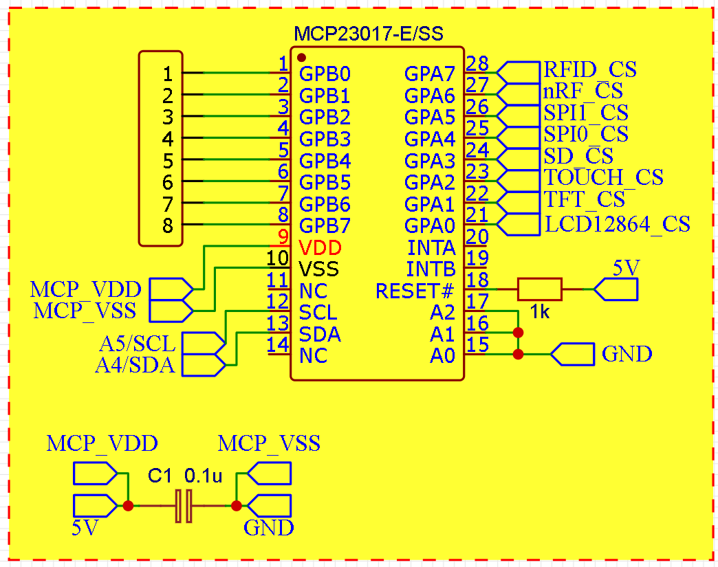
Now, what should I do with the mcp23017 spi pins ? For example, does the mcp23017 require a CS pin or it doesn't matter ? also what about if I want to read data with MISO ?
For SPI, you will need the MCP23S17, not the MCP23017 and you can ignore information that is specific to the MCP23017
If you only have one device on the SPI bus, you can hardwire the CS to GND; but if you ever want to expand with another SPI device (no matter which one), you have a problem.
They assume the input signals are open drain. Those need a pull-up resistor to work properly. But according to the Datasheet the PCF has internal pull-up current source which is much better than a mere pull-up resistor. Why TI decided to include weaker external pull-ups is mystery for me. I came up with two possible explanations:
No brain design. They see a possibly open drain output -> they add a pull up. They don't think about it long enough to realize it is redundant. IMO this is the right explanation.
Once I had a PCF (from eBay) with single damaged output pin: the current source was not working, the pin was only able to pull LOW. It took me some time to discover and debug. If I had an external pull-up this would be no problem. If it is known the current source is exceptionally vulnerable in this chip (which I doubt) the external resistors may be used as a fail-safe.
I think they don't use pull-ups for outputs for reason 1. - they didn't realize the pins are "pseudobidirectional" and OUTPUT HIGH is the same as INPUT_PULLUP (and it is unable to be input without pull-up).
Also note input to P5 makes no sense. The button connects the pin to another pull-up while it should ground the pin. As drawn pressing the button does nothing. Clearly TI didn't invest much effort in this schematic.
To your other questions: the MCP needs decoupling capacitors as well. All digital chips need some.
PCF has pin change interrupt capability too. In MCP it may be configured which pins trigger interrupt while PCF interrupts on any change in any pin.
There are two reasons for multiple filtering caps:
You make PCB space for various sizes and amount and populate only those needed and according to what is cheaper/available.
You may want to have a small fast capacitor parallel to a slower one with higher capacitance ("bulk") to cover various filtering needs.
I think 1. is what they had in mind because this simple IC hardly needs so much filtering.
For SPI, you will need the MCP23S17, not the MCP23017 and you can ignore information that is specific to the MCP23017
If you only have one device on the SPI bus, you can hardwire the CS to GND; but if you ever want to expand with another SPI device (no matter which one), you have a problem.
Yes, I'm thinking of using different SPI modules and I designed this circuit.
What you think ? Is it good ? I used 8 pins for on board spi modules and ported the other 8 pins for any other use.
If you are building a complex SPI-based system, why make it even more complex by using i2c bus also? It should be easier and neater to stick to one bus system. Could you use a humble 74hc595 instead of pcf/MCP chips?
Or, if you have 3 Arduino pins available, a 74hc138 ?


