i'm now working for a couple of weeks with the Portenta H7. Until my written code gets more complicated, i bought the breakout board and the ST-LINK/V2 to debug my code.
But i am a little confused by the wiring between the ST-Link and JTAG pins on the breakout board. I have read several times in the forum, that you talking about JTAG, but i think you mean SWD.
I have looked up the schematics of the breakout board and the schematics of the Portenta and i have come to the conclusion, that we can't use the JTAG protocol, since the JTDI pin (PA15 of the STM32H747) is used for communication with the WiFi module. Also the test reset pin nJTRST isn't connected to the JTAG connector of the breakout board. The nJTRST pin is pin D3 from the SD card connector.
So my question, if we want to debug the Portenta we always use the SWD protocol. Is that correct?
The last point is, how do you connect the ST-Link to the brakout board. Do you just solder some cables to the pins or is there a ready to use connector.
That's the problem with the portenta! Just nothing works! Everything you touch makes problems, JTAG connector, PWM, DMA,...
And the documentation is crap!
Why do other boards work fine and the Portenta does not? As eschi said, you even don't know how to connect JTAG, because it's not documented and you can't buy a cable without DIY. That's not PRO!
FYI: I agree with you: having a nice (HW) debugger working on Portenta H7 (besides just this Serial (UART) bootloader - without any debug, using Serial.println() is NOT debug) would be great.
With the breakout board - there is an access to the SWD pins. Without: the MCU module has some test pads on board (schematics) where you could solder SWD wires (very delicate but possible).
It works for me to connect ST-Link to Portenta H7. I can read and write (entire !) flash.
Just be careful not to overwrite the bootloader (0x08000000 ... 0x08040000). Otherwise the UART based flashloader will not work anymore.
Just to figure out (for me):
How to configure IDE (e.g. VSMicro) to use my ST-Link for a real HW debug (with breakpoints working). I think I saw that ST-Link used to flash works but not yet to debug (with step instructions).
I am pretty sure you can use a real HW debugger (ST-Link, Seeger). Just to figure out how to configure IDE.
We had to spend time to "debug the IDE": and Arduino, Portenta H7 team ..., could be more helpful/responsive (instead to let "US" to make it a professional system). LOL
I use JTag or SWD debuggers so rarely (about twice a decade), I have completely forgotten most of the steps. I have a few bricked Portenta's which I should re-burn the bootloader. Any suggestions?
I really like the bottom Particle Debugger as you connect the SWD, V and GND and drag the bin file to the pop up folder and that is it. I think my old steps are here
Anyone got any opinions of the easiest way? I have found where the official v23 Portent versions are here
Most of my Portenta's have just lost their serial connection. Is there an easy fix? Last time I just loaded the Arduino IDE (both old and new) up on multiple windows and Linux computers and one it finally worked, so I loaded a sketch and Serial connection restored.
If you have the Portenta H7 breakout board - the debug interface (signals) are easy to access. It works for me to connect there a SWD adapter (I use ST-Link).
If you have just the MCU module itself: you can still access the SWD signals (SWDIO, SWDCLK), but just via very tiny PCB probe pads. Potentially, you could solder wires there and connect.
Yes, if your bootloader is broken (e.g. lost from flash) - the only option is to flash it again with a real SWD debugger. (it worked for me, also a broken board).
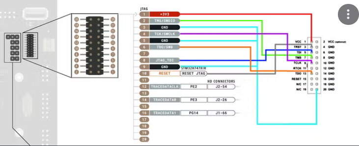
I have both the breakout board and the vision shields so I do have access to the JTAG pins. I am a bit confused by the number of pins. Wonder if anyone has drawn a diagram to show how a normal ST-link connects to it.
It is enough to wire just the SWD interface.
The signals needed are:
SWDIO
SWCLK
RESET - needed to use HW_Reset on ST_LINK
GND - for all signals as GND references
3V3, VDD - important! ST_LINK senses the target voltage!
Very important: my ST_LINK adapter SENSES the VDD on target board:
the 3V3 on JTAG header is an output (not to feed the board!): the debugger wants to see the
voltage there. If no voltage - it will not connect (assumes the target is powered off).
You do not need the other JTAG signals (SWD vs, JTAG mode).
And SWO is just needed for SWD Trace or when you use SWD Viewer (e.g. print via SWD)
(yes, you can print via debug interface, ITM_Trace)