Problem in a relay pcb card

You find below the pcb of a relay card that i had designed with Altium Designer, And right now i'm trying to test it but i have some issues :

  • Not all the relay card activated when i put GND in the inpout.
  • i think i have some issue and problems in the schematic
  • i think i had an errors in the components choice.
    Can you please give your feedbacks or any solution?
    Thanks a lot?.
    Relay Card Files.zip (1014.0 KB)

the PCB layout :


The Bill of materials :

why you using optoisolators when anyway all is powered from same 5V?

To ensure electrical isolation, I found that most relay board schematics use optocouplers. Do you have any recommendations?

The zip file will not open.

It would help people to help you if you put your schematic in your forum post, not as something people have to download. Please create a jpg image and upload that to the forum. Please list the components in the forum for the same reason. Also the PCB layout from Altium Designer.

Your schematic shows the external connector with 'Vcc', but everything on the board is powered from 5V, not Vcc. How is the 5V derived from Vcc? Maybe that's the source of your problem.

Have you measured the change in voltage across the relay coils when you ground the input to their associated opto isolator? What do you see on a good one and a bad one?

Some photos of the board would help, clearly show the components and the soldering.

  • We need a better resolution image of the schematic and PCB.
    Show us a PDF of both.

  • Why are the PCB traces so narrow ?

  • Do not see the Emitter to GND connection.

  • Your Opto Isolator does nothing for you.

  • (5v(Vcc) - 1.8v(led) - 1.3v(opto)) / 1k = 2mA
    This is not very much current :thinking:.

2 Likes

Hi, @alarmidaa

Did you bread board your design before committing to a PCB?

Do you have a DMM? (Digital MultiMeter)
Use it to trouble shoot your PCB.

Then use the working relays as a comparison to the non working relays with the DMM.

PS, Did you export or screen capture your PCB and schematic?

Your tracks look to thin as well as the PCB holes for the relays.

On your PCB I cannot see any gnd connection to any of the BJTs.

Tom.. :smiley: :+1: :coffee: :australia:

because it designed for alternative powering of transistors and relays, but in your schematic power lines are not splitted.

I would make this way:

The Schematic PDF is here:
RelayCard.pdf (348.1 KB)

Those bright green leds in series with the optocoupler leds may give you a problem. The forward voltage is up to 2.5 volts. https://www.farnell.com/datasheets/1854088.pdf

EDIT
If you had used blue leds instead of green it would have been even worse. There the forward voltage is up to 4v https://www.mouser.ch/datasheet/2/216/APT3216QBC_D-77006.pdf

1 Like

You need to eliminate the LED in series with the opto coupler. You can place that LED and a series resistor across the Relay coil.

  • Yes, that’s a much better location for the LED.

  • As is, the Opto-Isolator and BJT should replaced by a MOSFET, or properly incorporated.

Hi,
For all to see, @alarmidaa schematic of relay circuit.

Please look at post #7.

Tom.. :smiley: :+1: :coffee: :australia:

  • And what it could have been.

I know it is deviating more from the original issues raised by the OP but since we are redesigning it for him, here is another variant: PCF8575 cannot control relay switching - #13 by 6v6gt . It uses a clever design with an (AC) optocoupler that allows individual configuration of trigger high or trigger low on each channel.

1 Like
  • Yes I like that.

1 Like

Hello PerryBebbington,

Thank you very much for your comment. It is really helpful, and I appreciate it a lot.
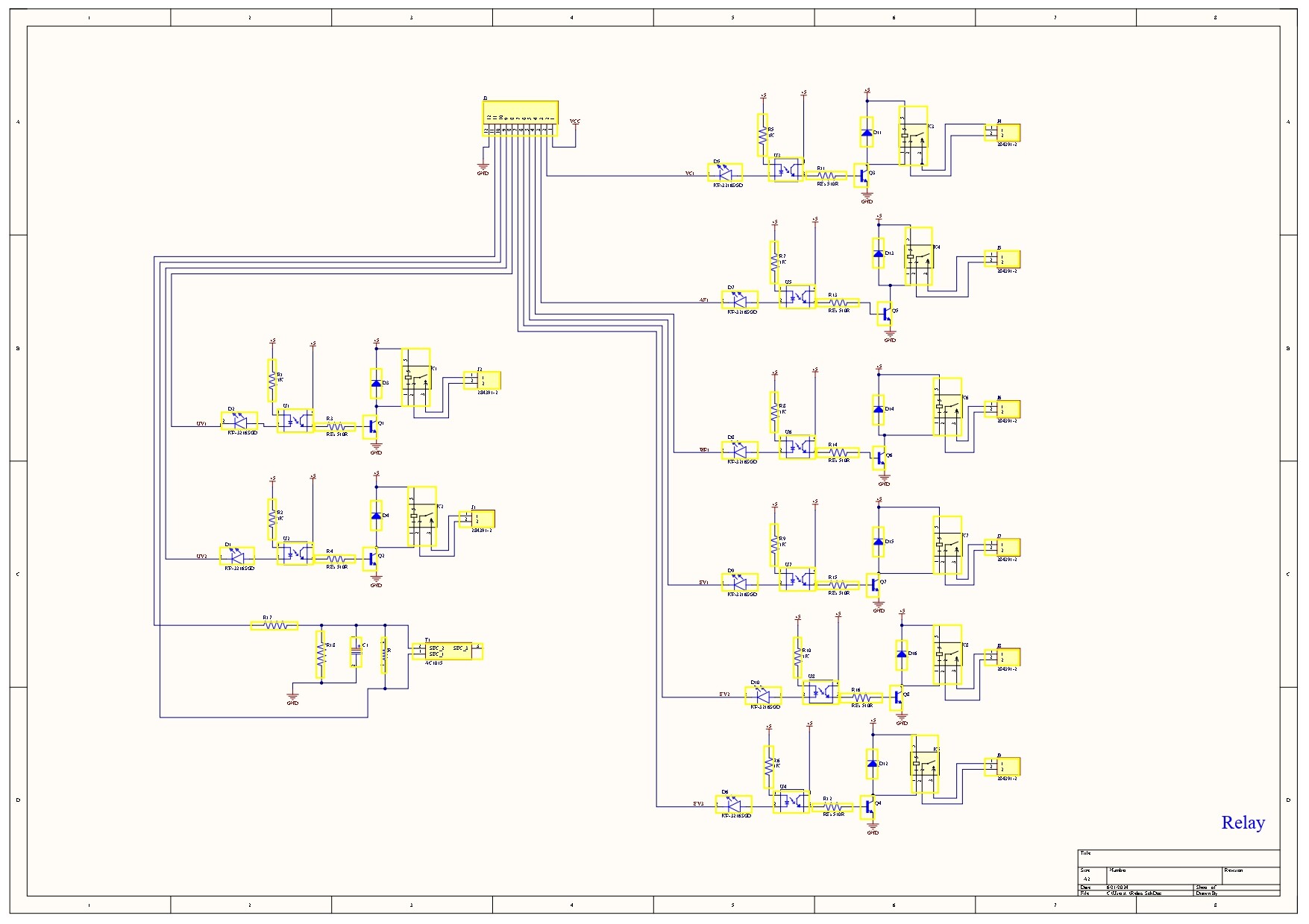
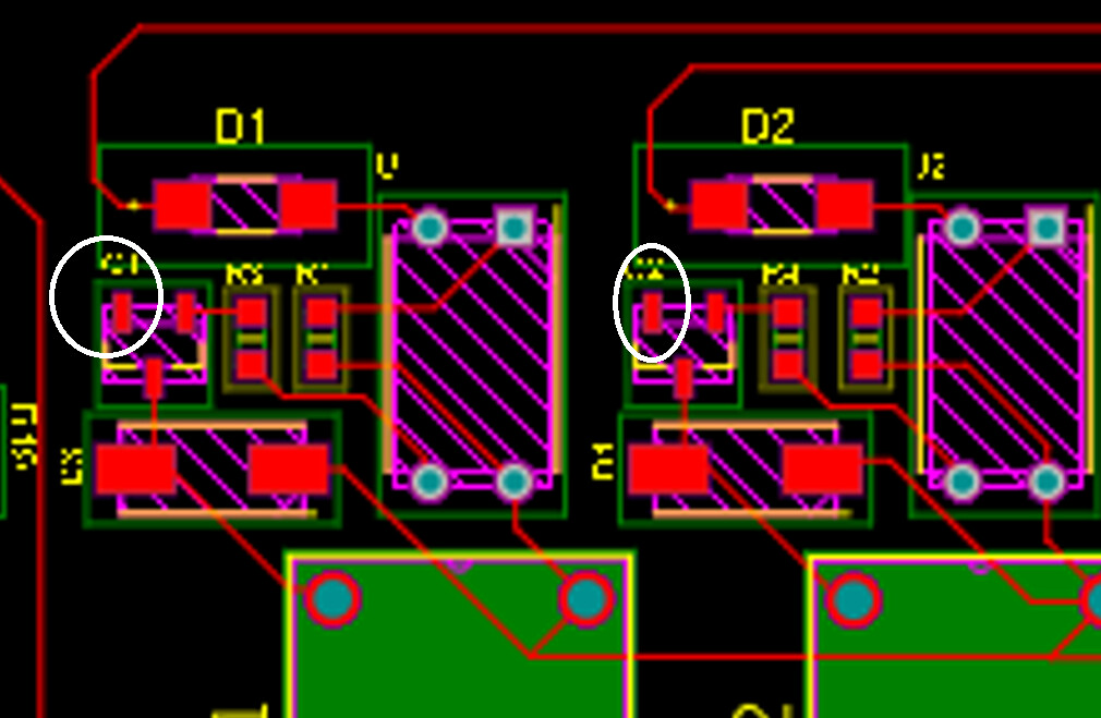
I have added the schematic, the PCB layout, and the Bill of Materials in JPG format.
Regarding the Vcc and 5V, they are the same and are connected to each other on the PCB.
As for the voltage of the optoisolator, I found the following:

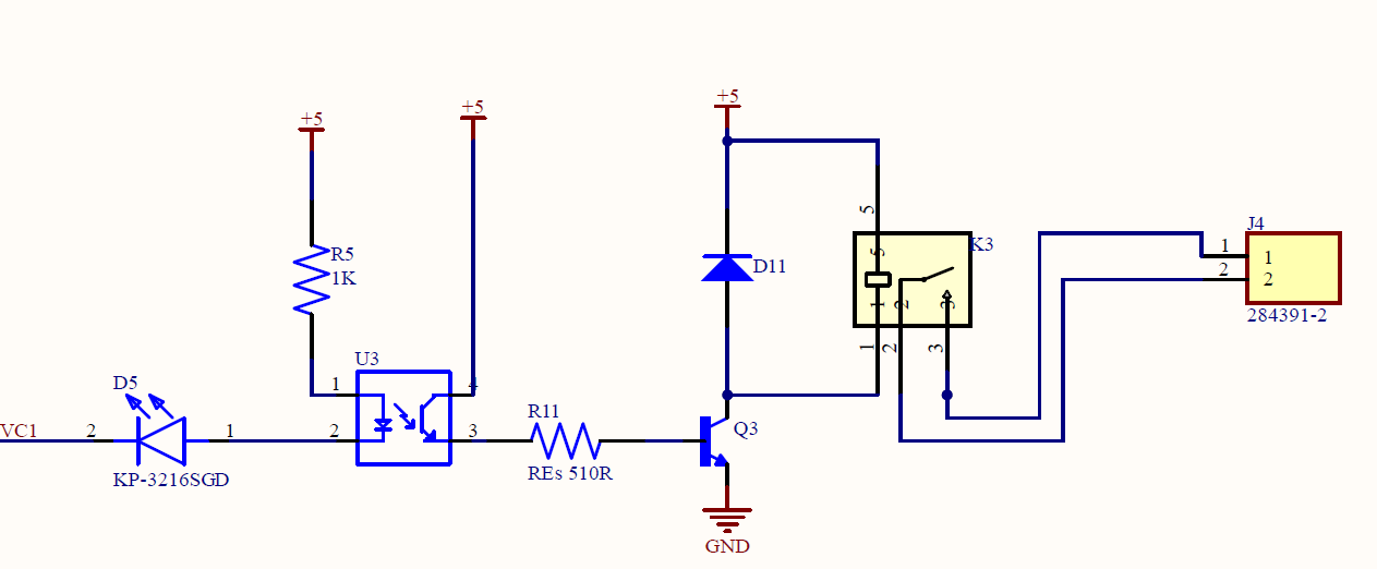
For K1 and K2 (the good ones), Vce = 2.28V
For the relay K3 (the bad one), Vce = 0.12V

1 Like

Between which points did you measure these voltages ?

EDIT
Have you made any changes between the circuits which work and those which don't. For example, even changing the colour of the LED could make a difference.

Sorry but please do this in a new post, by editing the original you have made to thread very confusing to anybody who wants to use this to solve a similar problem.

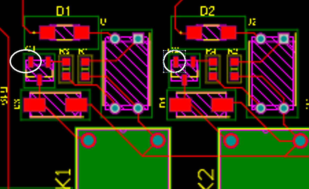
Have you seen the problem with your PCB, Q1 and Q2 etc, their emitters do not appear to be at gnd.

Tom... :smiley: :+1: :coffee: :australia:
PS. Are you posting screen captures or EXPORTED jpg from your CAD, the resolution appears very low.

This topic was automatically closed 180 days after the last reply. New replies are no longer allowed.