Nice, that's a free feature ![]()
Well that rules out anything I could come up with.
Now that I think about it....
If you look at the power supply circuit of my first post, maybe the 12V right before the LDO are clean enough to drive some mosfets with it? ![]()
OK!
Nope; you don't need a particularly clean power supply, and there are plenty of MOSFETs that will be switched easily with 5V or much less. In fact, the MOSFETs you started with in #1 fit the bill.
It might be there to protect the switch from reverse polarity in an automotive environment. It's OK to add it there if that's the reason. Do understand though that in case of e.g. a reverse-connected battery, it may start a fire.
I really doubt it.
If the MOSFETs need 5V Vgs and the source voltage is 12V, wouldn't you need 17V+ on the gate? Can the driver pump up 17V from 5V? Maybe you should supply the driver's Vcc with 12V.
After reading and considering all posts I think I have two options to follow.
- Finding something like the VN7004, but PWM controlable.
- Utilizing a MOSFET as a low side switch.
Option 1 should be the easier way regarding designing it, but only if I find the right part.
Option 2 looks like the better, more conventional way. Sadly I don´t have any experience in controlling a MOSFET with 12V using a 5V microcontroller (I now this is a dumb description).
Does someone has an schematic as an example?
As I said, I´m more of a mechanical engineering guy, so if you have questions about how to repair your car or bike, feel free to ask ![]()
Can you isolate the negative side of the fan from the chassis
Yes, no problem. Most fans don´t have a chassis ground, so two wires.
2A: use an N-channel MOSFET as low-side switch
2B: use a P-channel MOSFER as a high-side switch.
Both can be PWM driven if needed.
If you use a low-side switch, you don't control the MOSFET with 12V. You control it with whatever Vgs is needed to turn it fully on. For a logic level MOSFET, this can be 3.3V or 5V.
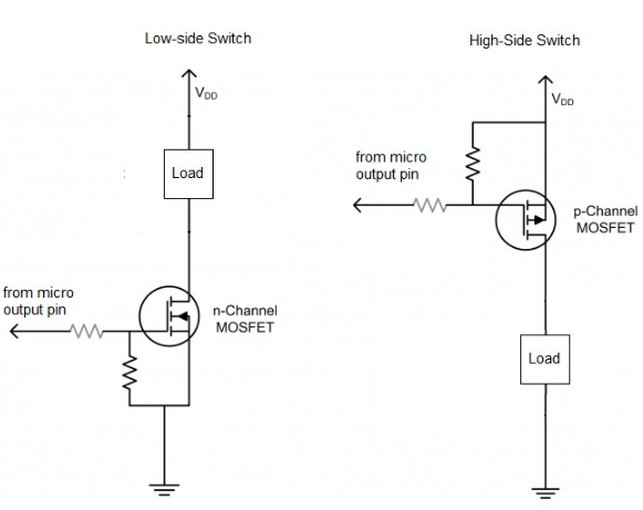
Left: low-side switch using N-channel MOSFET. (but put the gate pulldown to the left side of the grey gate series resistor)
Right: high-side switch using P-channel MOSFET.
Note that in the right-side example, the high-side switch, your objection/concern is justified since the gate needs to be pulled up to Vdd (12V in your automotive case) and then pulled down by a few volts. Since you can't connect a microcontroller GPIO to a net that's pulled up to 12V, you'll have to make an intermediate step:

Here, you use a small-signal MOSFET such as BSS123, 2n7002 or even an NPN like BC847, 8050, 2n2222 etc. to pull down the gate of the big P-channel MOSFET that acts as the high side switch. This allows you to drive the P-mos' gate that floats at 12V (or even much higher) from a logic-level GPIO (3.3V or 5V).
The P-mos gate pullup R3 can be pretty much anything, but usually something like 100k or even bigger is used. It's a tradeoff between dissipation in this resistor vs. the time constant of the P-Mosfet's input capacitance. Long story; don't worry about it for lowish PWM frequencies of maybe a few kHz.
The low-side N-channel switch doesn't have this limitation because the gate doesn't ever have to go all the way up to 12V.
Thank you very very much for this nice explanation/example.
So I think 2A it is.
You said that the MOSFET I´m currently using would do the trick. I want to switch to the MOT100N02D. Much easier to solder ![]()
How do I calculate if a driver for the MOSFET is needed? And what values should the resistors be? Or how do I calculate that?
I can't find a datasheet for that one. Do you have a link?
You generally don't need one for option 2A. Pick a logic level MOSFET that can be driven directly from a GPIO.
Not very critical; I generally use something like 100k for the gate pulldown. The gate series resistor isn't particularly critical; I like to use something like 160R because this keeps the current through the GPIO quite low in case something goes wrong on the gate side, shunting it to GND. Not that this would typically happen, but it's nice to feel safe.
I could make a really complicated argument about selecting these resistors, but the conclusion would be that in your application, it won't make all that much of a difference anyway. They're just not critical.
Here you go:
I really like to hear that ![]()
If you are switching 30A on and off you need to do it as fast as possible, otherwise your switching losses could be higher than your ohmic losses. 20ma from an Arduino pin just won't work with MOSFETs with large input capacitances.
Do you have a hot air reflow station for soldering?
Ok, where would be the limit in capacitance with the standard PWM frequency?
Yes, I got a reflow station, and a Chinese soldering oven.
Has nothing to do wih PWM frequency, it how long you take to switch from completely off to completely on and then back
Thanks; looks good. Keep in mind that even at a lowish 6mR of Rds, at 30A you're still looking at serious dissipation figures.
Yes, it does. The time spent in the ohmic region is larger at higher PWM frequencies. As a result, frequency matters massively when driving MOSFETs with high Ciss. It makes the difference between pyrotechnics and electronics. A gate driver will help reduce the problem. Frequency still matters.
You can calculate it, but it's a chore. More sensible is to simulate it in SPICE and then make a judgement call based on the results of the simulation.
Yeah, you are right.
At 6mOhm and 30A it would be around 5,4W of heat. Thats why I used two MOSFETs in paralell in hopes to lower that heat.
I never used SPICE, I will look into that.
Don't expect both MOSFETs to turn on and off at the same time, especially when you need to do it very fast
It's neat, but there's a learning curve. I use LTSpice which is free to use, but the interface is from the 1990s. It's very powerful, though.
Here's a quick sim of a low-side NMOS switch:

It's the same circuit, with the only difference between that the left one is driven at 1kHz and the right one at 10kHz. The plot at the top is the dissipation in the MOSFET. The peaks occur when the MOSFETs are between on-and-off, so the transition period as the gate is being charged by the driver (and then discharges at the end of the on-period). I modeled the driver to have a series resistance of 500R; at a 10V amplitude, this means max 20mA of drive current.
The numbers aren't too important; what I mean to show with this is that you can get a 'ballpark idea' of what's happening - and that in this case the switching losses are very significant, especially at higher PWM frequency: just compare the total area below the green plot vs. the blue plot.
I chose the IRFP2907 because it's a bit of a worst-case scenario; it has an input capacitance of 13000pF; this is about 4 times as high as the MOSFET you chose. Then again, I simulated with a load current of 'only' 12A. The net result will be a bit less problematic for your circuit under the anticipated conditions (500Hz PWM frequency).
Keep in mind that if you drive two MOSFETs, the drive current will distribute over both of them, so the switching losses will increase if the driver is feeble (microcontroller GPIO). I'd sooner opt for a more suitable MOSFET and keep it a single one.
Thanks for the quick simulation and the insight.
So, if I use a driver that is capable of more than 20mA, I can reduce switching loss drasticly?