vlachoudis:
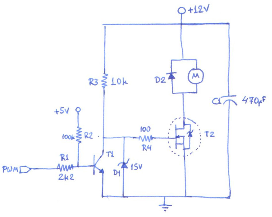
Thank everybody for the suggestions. Indeed the R1/R2 wrongly perform a voltage divider, luckily it was giving always a Vb=.1V<0.6 so the transistor didn't turn on. I moved the R2 on the left of R1 and reduce the R1 to 1k.
Also reducing the R3 to 330 and suppressing the R4 the MOSFET goes high immediately giving a "nice" square pulse. With the R3=10k as it was it had a slow rise of 40us. I have prepared also a 555 as monostable and I will check on the weekend on the kart how it performs and report back here.
@TomGeorge I do have a fuse of 30A which didn't blew up 
That is because your problem wasn't over current, it was the slow switching time. R1 and R2 had nothing to do with it, and were perfectly fine just as they were. The problem was R3.
When using a transistor as a switch, broadly speaking there are 3 states it can be in.
The first is cutoff. Just like the name implies, the transistor is "turned off" and not conducting current. This is when voltage is at maximum, and the current is at a minimum, just a small amount of leakage. Ideally, it would be 0. High voltage * very low current = low power dissipation, so low heat.
The second is saturation. This is when the transistor is "turned on" and conducting current. The current is it it's maximum value, but voltage will be at a minimum. High current * low voltage = also low power dissipation, just like cutoff.
The transistor cannot immediately and perfectly transition between those two state. As you reduce the driving signal from saturation, the voltage will gradually fall and the current will gradually rise. During the transition, with the voltage and current both having significantly large values, there will be significant power dissipated by the transistor. The same thing happens in reverse when increasing the drive signal from cutoff: the current ramps up and the voltage ramps down, leading to a similar pulse of power.
This region between saturation and cutoff is called the linear region, and is a very bad place to be for a power transistor. You want to spend as much time as possible in saturation and cutoff, and stay out of the linear region. Unfortunately, whenever you transition between cutoff and saturation, you have to pass through the linear region. You cannot avoid it, and you cannot reduce the peak power of the linear region's pulse.
The one thing you can control is the amount of time you spend in the linear region. Power is energy per unit time, so if you spend less time in the linear region, the circuit will dissipate less heat even if the peak power is the same. It's like the relationship between speed and distance. Even if you keep your speed the same, you can change the distance you travel by changing the amount of time you move for.
This is why I said that your observation that the failure happens during acceleration clinches it. PWMing the MOSFET will cause it to make very frequent transitions through the linear region, around 1,000 times per second at the default PWM frequency. Increasing the frequency to 15 kHz does not help, it actually makes it much, much worse. In the worst case, the low-pass filter caused by the resistor and the gate capacitance will cause the MOSFET to stay in the linear region causing constant power dissipation. This will not happen when the MOSFET is held fully on or fully off, because then there are no transitions through the linear region causing excessive power dissipation.
This is why the gate driving circuit is critically important for high-powered MOSFETs that will be rapidly switched. There are even specific ICs called gate drivers that are specifically designed to switch MOSFETs as rapidly as possible with high current pulses, some of them rated for several amps. A 10A gate driver will fully charge a 1 nF gate to 10 V in 1 ns.
Decreasing the R3 resistor from 10K to 330R is a legitimate solution that will increase your gate drive current, allowing you to spend less time in the linear region. However, it also consumes more power because turning off the MOSFET requires connecting it straight to GND. 12V/330R = 36 mA being wasted when the MOSFET is help off. This may or may not matter depending on how much room you have in your power budget.
I have prepared also a 555 as monostable and I will check on the weekend on the kart how it performs and report back here.
The circuit in Terry's link is not a monostable configuration, nor is it an astable configuration, which is the other way the 555s are normally used. It is using the 555 as a current buffer in order to take advantage of the relatively large amount of output current (100-200 mA) that most 555 chips are capable of driving. It's basically just a stand-in substitute for a real gate driver chip.