What is the peak voltage you expect, and peak current? That are two parameters you need to size your MOSFET.
Just looking at your proposed schematic again, you use an optocoupler to get the input voltage (100-200V or so) to the gate of the MOSFET. Bad idea: the maximum allowed Vgs of the IRL630 is 10V. That high voltage on the gate will kill it. Other MOSFETs will have higher Vgs(max) rating but its nowhere near the voltages you want to apply.
You could make a voltage divider with R1, R2 and a pull-down resistor on the gate (which is missing from your schematic) but that only works reliably when you you have a fixed high voltage. You're planning to regulate this.
You'll need some kind of fixed voltage supply to switch your MOSFET gate.
that waveform looks easy enough to produce on an Arduino output.
Set an interrupt to trigger on the zero detection.
That interrupt sets a timer interrupt to switch on the signal.
When the timer interrupt is triggered, set the port (direct port write, digitalWrite() may be too slow) and sets the timer again for 2 ms later.
When that second timer interrupt is triggered, switch off the signal, and wait for the next zero crossing.
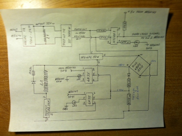
Thank you to all of YOU for trying to help me.Dear "wvmarle" I do not know how to write the cod for Arduino. I try some programs written on ARDUINO playground, but no success for now. After reading all suggestion I came to a new schematic which I will attach . Could you please check it and if you think it will need some changes to work, please give me your opinion.If you think the schematic will work I will really appreciate if some of you write and send me a code to upload on my Arduino
dgueorguiev:
Thank you to all of YOU for trying to help me.Dear "wvmarle" I do not know how to write the cod for Arduino. I try some programs written on ARDUINO playground, but no success for now. After reading all suggestion I came to a new schematic which I will attach . Could you please check it and if you think it will need some changes to work, please give me your opinion
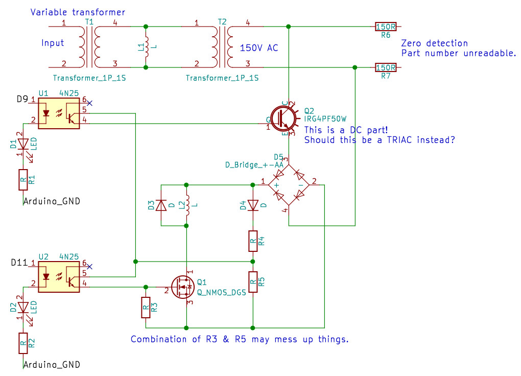
At L2 there's a flyback diode, that's good - make sure it's a type that can handle the current. A common 1N4007 will do fine. But you should not add that resistor there, as it completely negates the purpose of the diode which is to provide an easy path for the reverse current to flow.
The 4N35 optocouplers: why is there an LED in series? Any purpose for that? Also they miss a current limiting resistor.
Why two of them? You just need a pull-down resistor there. But it's getting tricky with the extra voltage divider. That one has the wrong values, 10k & 8750 Ohm is not going to divide 150V into (140+10)V.
The MOSFET: the Irf9z24n is a p-channel type. You need an n-channel. Also maximum VDS is 55V while you have 150V.
.If you think the schematic will work I will really appreciate if some of you write and send me a code to upload on my Arduino
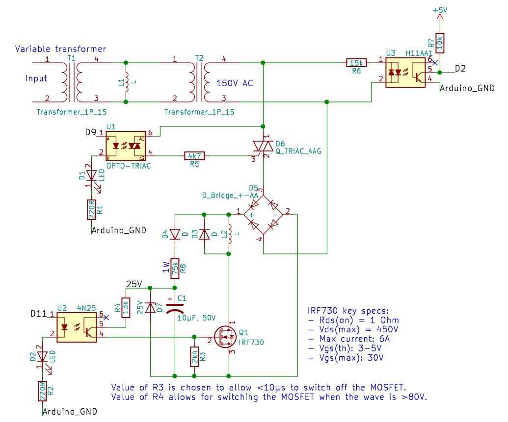
Added the missing resistors for the optocouplers and the MOSFET.
Can't read the part number for the phase detection, so didn't add that.
The IRG4PC is some kind of transistor, I'm not familiar with this special kind, but it seems to be a DC part that you put in an AC role. It will break right away as the reverse voltage is just 18V according to the data sheet and you're going to apply 150V AC. I think you want to use a TRIAC there. Your phase diagram in #24 suggest this:
The IRG4PC is an IGBT, but the Op has the driver for it completely wrong plus the IGBT has a recovery diode from C to E so it will fully conduct on the negative cycle.
IGBTs do not like AC current.
Another thing, that H11AA1 opto. I just checked the spec sheet, so now I know how that works. It switches off for a moment every time there's a zero crossing, so that's easy enough to detect.
There is no need for a resistor in both lines, one of R6 or R7 can go.
Then the value. At 150V and total 300 Ohm you get 500 mA. That'll burn the LEDs very fast. A good forward current is 10 mA, at a drop of 1V over the LED (negligible on a total of 150V) that would require a resistor of 15k. So not 2x 150 Ohm.
Then we have to find proper values for the R4/R5 voltage divider, with it the R3 pull-down.
For that, we need to select a good MOSFET Q2, and a replacement for Q1 - a TRIAC. I don't recall any current ratings by OP for these parts, which is needed to make a selection. Fast switching is a requirement (for accurate timing - target <1 us), so gate capacitance becomes important (in combination with R3, R4 and R5).
Well, OP, I think you have your homework here. Looking forward to your input.
Playing with this schematic again, another problem. The LED at the output of the H11AA1. It can not light up, ever (due to far too little current flowing through the 10k resistor), but together with the optocoupler it will prevent the voltage to drop low enough: about 1.8V for a typical red LED plus 0.4V for that phototransistor means the output voltage will vary between +2.2 and +5V. That +2.2 will not reliably register as a LOW.
I've replaced the IGBT for a TRIAC. That should at least work for switching the AC to the rectifier for L2.
Now I don't really understand how that TRIAC can switch on a DC supply, unless you want to switch only half the time. For switching the negative cycle it seems to need a negative pulse, and that's not provided here. So it won't work. When looking for Arduino/TRIAC circuits an optotriac is used. So all that brings me to this circuit diagram:
The zener is for protection of the MOSFET gate. The values as chosen for the voltage divider will allow about 1.5 mA of current to flow, resulting in 15V on the gate. The zener I set to 12V, may change that to 15V or so.
Just realise that I'm calculating at 150V for the DC which of course is wrong as the peak value is much higher, about 210V. However the moment the MOSFET has to switch, the voltage in the circuit is below peak, so we must keep that in mind as well. Maybe a bigger pull-down resistor is needed so the MOSFET can properly switch on when the wave reaches 100V or so (the current requirements are not like that but it's easy to allow for it now, hard to change after building the circuit).
Another question: what is the purpose of this TRIAC switch? It doesn't seem to me that it adds anything to the switching of that coil L2, which is switched fully by MOSFET Q1 already. I don't see any additional effect of it, except adding some serious complexity.
OK, and now I should stop playing with this It's a good exercise.
MOSFET I chose the IRF730 for sufficient voltage (500V) and 6A max current. Hope that's enough.
Based on that recalculated the resistors, keeping in mind that we'd want a 10µs switching time for the MOSFET. This results in a 20k, 5W resistor for R4.
Checking the data sheet I also noticed the 4N25 optocoupler is not suitable for this application as the breakdown voltage is 70V, and the peak wave here is more like 210-220V. So this needs a different part, one that can handle 300V or so.
wvmarle:
OK, and now I should stop playing with this It's a good exercise.
Checking the data sheet I also noticed the 4N25 optocoupler is not suitable for this application as the breakdown voltage is 70V, and the peak wave here is more like 210-220V. So this needs a different part, one that can handle 300V or so.
Keep going.
Split R4 into two resistors in series and connect a zener to the midpoint and MOSFET source, that way you have a zener regulator.
To keep Vmax to the collector below 70V of the 4N25, add a 10uF or so to give you some smooth gate voltage.
Tom...
Good idea. That could also help solve the massive 5W heat dissipation. The on switching is the real issue, I was thinking already of adding a cap somewhere to help giving that MOSFET gate a good push to get on.
Zener D7 limits the voltage over the cap to 25V. Every time the voltage goes over 25V on the rectifier (or over 150V if the optocoupler is on) the cap C1 will be topped up to 25V. Then when the optocoupler switches on, there's this 25V supply from the cap to help switch on the MOSFET faster. D4 prevents back flow from the capacitor when the wave goes below 25V.
The zener also manages the CE voltage of the optopcoupler.
OK ,you spend to much time for me.Thank you so much , but I have some more details:
What about if I lower R7 from 10K to 2.2K? Do you think it will work better for "0" crossing signal to Arduino?
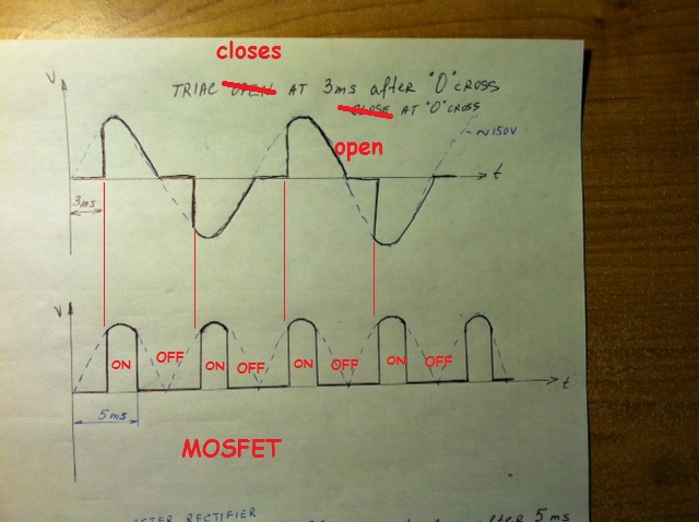
The idea for TRIAC is to open 3ms after"0" crossing and close at next "0" crossing, by itself. This will cut off first1/3 of half AC wave. ( I order TRIAC T-835H-6T) and (optoisolator triac driver 782-IL410 ). Modified AC after full wave rectifier bridge "+DC " go trough Mosfet ( I order logic mosfet IPP200N15N3G) ,which will open at "0"cross and close 5ms. after that. the overlap of open circuit will give me 2ms pulses I need. May be there is easy way to achieve this goal, but I am not aware.
I order zener IN5253 .Is this correct? If not can you help me with new part number and the place to order
Look like We are close to final view of the schematic. Can you help me with programing cod for the ARDUINO board? I have ARDUINO UNO board. And I have no idea how to write the program.
Thank you ones again. You are amazing !!!
Dimitre
Hi,
We were puzzled as to why you needed the Triac to start the waveform.
You don't need it as the MOSFET can do the switch ON and OFF, as the MOSFET is switching a DC supply, even though it is pulsing.
All your timing is referenced to the zero crossing detector.
After posting I was thinking about my schematic again, and realised that as R3 and R4 are forming a voltage divider again, gate voltage will be limited to <4V with my suggested values. That doesn't work (plus the rise time of the gate is much too low).
The solution I was thinking of was to add a second optocoupler, in parallel with R3. Then R3 value can be increased drastically (to 220k or so) as it's main purpose is to keep the MOSFET off upon startup. R4 value can be lowered then, zener can also go down a bit, 15V would be fine.
The purpose of this is to make the switching as fast as reasonably possible - the fastest is to short the gate to either the higher voltage or the lower voltage: that's basically what those two optocouplers do. Well, with a current limiting resistor to keep things under control.
The reason of going to these lengths: you want the MOSFET to switch at specific points of the waveform, for a period of 2 ms. A delay of 20 us is 1% of that time, and that will start to influence any measurement you want to do. You must try and minimise this delay as much as possible.
A serious complication is the high voltages you have. You're delaying with about 210V peak, while the MOSFET can have no more than 30V on it's gate. So I'm looking to find a way to "kick" the MOSFET into on and off states respectively, providing the required 20+ mA to charge/discharge the gate which is needed to ensure fast switching.
Wrong part - your RMS is 150V so that means peak is more like 210V. Also running it at the limit is not a good idea, you may have voltage spikes. That's why I came up with a part that allows up to 500V V(DS).
Furthermore, it feels not very "logic level" when I read the data sheet. R(DS,ON) values are given for 8V and more. The graphs later also show very limited conductance at 5V V(GS). Now for this application you don't need a logic level anyway, as you have plenty of voltage available.
The maximum V(GS) for this part is 20V so that's another mismatch. If after fixing the schematic I posted you manage to get the full 25V of the zener to the gate, you'd destroy the part even before you blow it with the too high V(DS).