Redesigning PCB for Surface Mounted components

Hi guys,

I designed a PCB using EasyEDA a year ago and finally just managed to finish my arduino code. Instead of a single arduino Nano Every, I now need the NanoEvery to send its data to the ProMicro which will act as a USB davice to forward MIDI information.

The goal is to surface mount all of the components that previously had their own daughter boards, which are the Rotary Encoder, Arduino Nano Every (ATMega4809) and the ProMicro (ATMega32u4).

I wanted to start with replacing the rotary encoder with a surface-mountable one and already have my first few issues/questions.

First of all, I cant seem to figure out the pin layout required, and the Datasheet isnt giving me the info I need either.

Old Encoder:

New Encoder:

I dont have a necessary requirement for this specific new Rotary encoder, other than it not having a daughter board. That said, EasyEDA only had this single one available in the "JLCPCB Assembled" list. My understanding is that these components can be surfacemounted in china while the PCB is being made - saving me the work of soldering on the components. Can anyone confirm this?

In addition, will I need any resistors? If so, where and what kind?

Any help would be greatly appreciated.

What makes you think the push switch should connect to Vcc? :roll_eyes:

Graphs like this.
image

From your comment I assume 5V isnt required then and I can just connect pins "2" and "C" both to Ground?

Yes. You seriously need to ignore such schematics by rank amateurs. :grin:

(OK, did you perchance get that from the Arduino tutorials? Also a poor source of information, sad to say. :thinking:)

Yes, but if you are going to use the same code, I want to know the details of your "old" encoder. It is most likely that the switch does connect to ground in it and it contains either two or three pull-ups to the "VCC" pin. You may need to add pullups to the new encoder or use INPUT_PULLUP on the pins.

Look at p2 of the data sheet and it shows the exact pin out and spacing. And the EasyEDA part at JLCPCB has the correct PCB footprint.
But, the PEC11 series are not surface mount components, they are through hole. JLC will do assembly, but you will have to pay a through-hole/hand soldering fee. Its not much.

Comparing the old to new (A and B are interchangeable, swap in code if needed):
CLK is same as A
DT same as B
SW same as 1 or 2.

Some modules will have pull up resistors already connected to the rotary and the switch.
The Bournes is a bare part. As @Paul_B said, your old module probably had pullup resistors.
When I designed my PCB, I went all in with resistors and capacitor for de-bouncing and pull up. Though if not doing hardware de-bounce (which I highly recommend since you are designing the PCB and those surface mount resistors and caps are dirt cheap) you would do input-pullup on D2,D3, D8. Pin2 (or1) of the PEC11 should go to GND, not VCC.

Also keep in mind that the data sheet p1 gives you all the info regarding what the numbers after PEC11R mean.

A tip: Click EasyEDA Library button. Select JLCPCB assembled, and then type in PEC11 as the search term. You will find many more, along with the footprint.

I remember the encoder being a pain to program (with the responsiveness and accuracy I wanted, without it skipping any numbers. Using some wacko math I found online to get it to work correctly).

I am currently using the following variables:

int rotarySwitch = 8;  // Used for the 'Rotary push button switch
const int rotaryCLKInterrupt = 2;        // Used for generating interrupts using CLK signal
const int rotaryRead = 3;                // Used for reading DT signal

In the Setup I set

  pinMode(rotaryCLKInterrupt, INPUT);
  pinMode(rotaryRead, INPUT); 
  pinMode(rotarySwitch, INPUT);

Is that what you mean, or am I missing something? Will This still work with the new encoder?


Yes, I looked at those images for ages yesterday but seeing that I dont even know if a switch needs power or ground, It didnt do me much good.

It seems like it. The Daughterboard the of the rotary encoder I have has some small resistors on the bottom.

I remember my rotary encoder code being super wacky and complex for what it is. The reason being that it wasnt stable or responsive. If you like I can post the rotary code here if its any help.

Regarding the PEC11 rotary encoder - is there any "right" or "wrong" one to choose? The ones in the list all have different part numbers, and I expect different specs. Are the differences of any relevance to me?

What resistors would I need to add, and where would they need to go?

This is my sheet so far:

Please look at the data sheet, page 1.
I think the most important question you have to answer are:

  • smooth movement or detents?
  • how many detents per full revolution
  • switch or no switch (I think your answer is yes)
    Look at How TO Order, and choose from there:
    4 1 15 F-S 0018 gives 18 detents, 15 mm long shaft, fluted shaft, with switch and 18 pulses per rev.

I will post a copy of my PCB design later if you like. It has all the resistor values, etc. I have tested it on my oscilloscope and have zero bounce :slight_smile:

  • smooth movement or detents? -> I havent tried smooth yet, might order one to test that,
  • how many detents per full revolution - I doubt it makes a difference if there are 18 or 24? (At least for my project)
  • switch or no switch - Yes, absolutely a switch. I use the switch to enter the settings

Thanks for the info, I'll try and wrap my head around this.
My brain was already overwhelmed with getting the code to work - choosing parts from millions of options isn't making it much easier :sweat_smile:

That would be very much appreciated!!!!

I have attached 2 circuits. The first one is basic de-bounce:
R1 is the pull-up resistor. R2 is to reduce the discharge current out of the capacitor to ground when a switch is closed. The exact values don't matter too much, but typically R1 of 10k and R2 of 1k to 10k work well.
C1 can be 0.1u to 1u. The larger number will give a longer time constant.

The second circuit has all the bells and whistles, including a Schmitt trigger IC (cheap) for sharpening up the output transitions.

Encoder Debounce 01.pdf (54.6 KB)
Encoder Debounce 02.pdf (105.2 KB)

If you have any questions about how to find the parts, let me know.
This video goes into some scope work:

Thanks a bunch for all of the help so far. I've attached a screenshot of the current design.
(FYI the NanoEvery is doing all the heavy lifting and sending MIDI info to the ProMicro which acts as the Native USB Device).

I still have two hardware issues I need to solve.

The first one is the OLED display. I'd like to mount it a bit more securely, but I dont want to mount it to the top-plate as that should only be added as a "beauty layer", and not add to stability.

This is how I currently have it attached (not very elegant - just floating in the air):

How would you normally go about stabalizing something like this?


And lastly, I want to add a USB-C connector to the PCB because IMO it's superior to USB-B or Mini-USB, and I dont want users to be plugging the USB cable directly into the Arduino. (It should integrate into the chassis I'm building, similar to the image below, just with USB-C).

I was going to use the following graphic To rebuild the curcuit. Seeing that my previous reference for the Encoder was completely wrong, could you please confirm that this connection diagram is correct?

Also, do you know what pins on the ProMicro need to be connected to the different pins on the USB-C connector? Cant seem to figure that part out :confused:

Instead of having to redesign the whole board why not use the existing design and use SMD to DIP adapters

Appreciate your posting the entire diagram. It helps a lot.

One correction:
The PEC_A_Out is the connection to the Every pin D2. The PEC_A is connected to the PEC11 rotary encoder. The same applies to the B and SW net ports too.

There are a couple of options for the OLED.
The hard way would be to find an appropriate module on JLCPCB.
The easier way, but still a little hard, would be to create a footprint for the OLED on your PCB and solder it in yourself:

  • Measure the mounting holes in the existing OLED (diameter and spacing)
  • Place pads on the PCB in EasyEDA with the above dimensions and spacing
  • Add a 4-pin header to the schematic (Commonly Library/Connectors, and choose 2.54 mm spacing). Place it on the PCB where the OLED 4 pin header goes
  • Double-check with 3D view to make sure that you really do have holes at the pads and the header
  • Do NOT order the header when going through the parts list at the final stage of the ordering process. This will give you properly placed holes for the OLED
  • Mount the OLED using short standoffs and solder the pins into the holes where the header would have gone. You may only need the lower two holes to have standoffs. Snip off the pins flush to the underside of the board.
    This is a lot more complicated to describe than to do :slight_smile:. It will give you an OLED display that is fairly flush with the board.

I think that with all this and the encoder mounted to the board, your project will look very nice.

In regards to @c-richmond suggestion, how are you planning on attaching the micros to the PCB? Using DIP sockets and plugging the micros into the PCB could certainly work.
Or as I mentioned for the OLED, if your Every and Pro-micro have male headers, you could put the DIP sockets in the schematic, place them on the PCB so that all your spacings are correct and just not or order the sockets.
If your micros just have holes and no headers, and you want to solder them in place, have JLC place male headers in the the appropriate places and solder the micros to the headers.

Is there a strong reason for not using the USB on the Pro? I am not familiar with the pin out for the Pro and where every thing connects internally. You may have to dig into that a little bit.

First of all, thank you so much for the continuous help. It means a lot to an absolute beginner like myself who barely knows what "PCB" even means! :sweat_smile:

Yup, totally forgot to rename them correctly after Copy/Pasting :woozy_face:
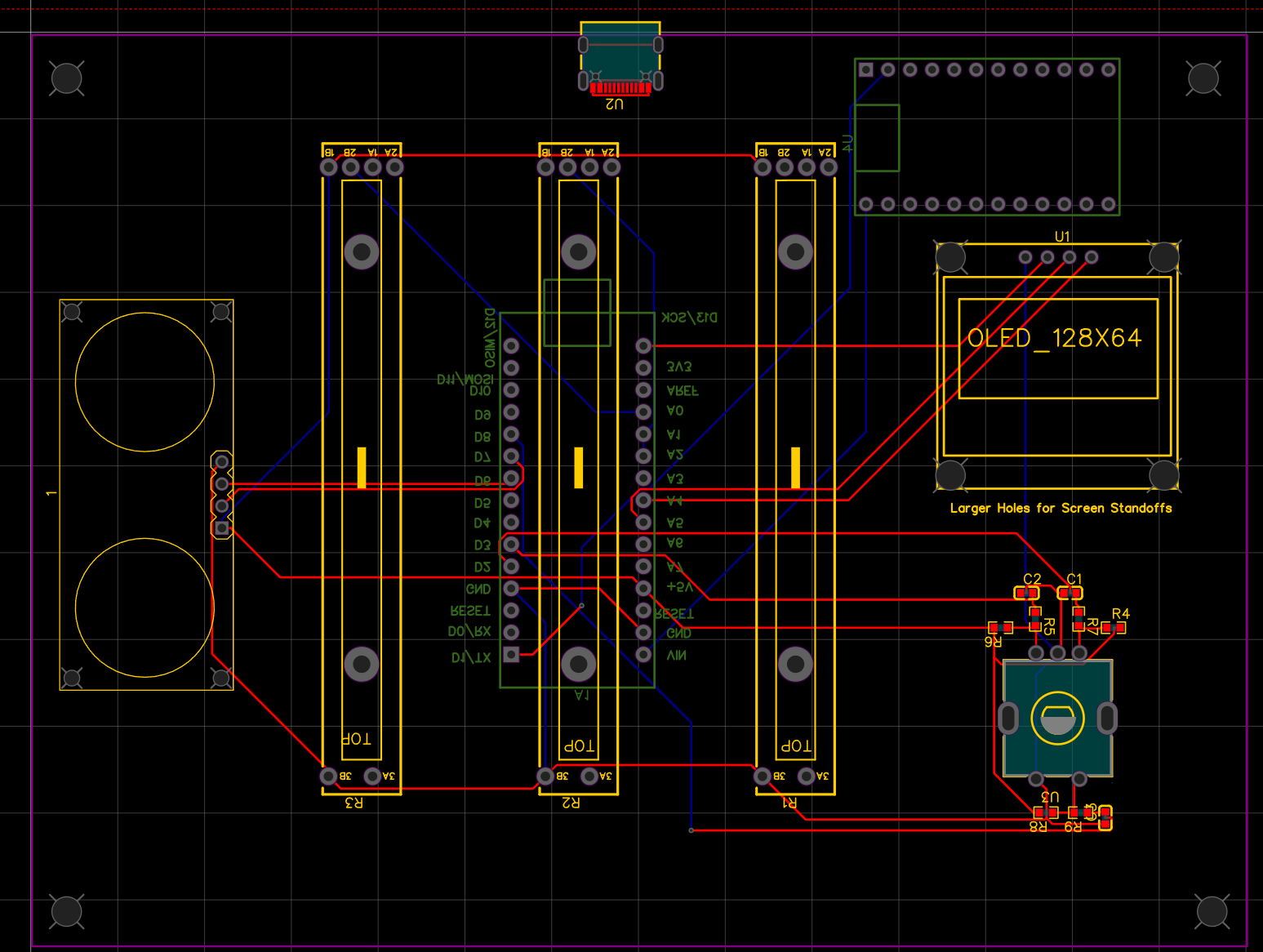
This should now hopefully be correct (?):


  • Measure the mounting holes in the existing OLED (diameter and spacing)
  • ...

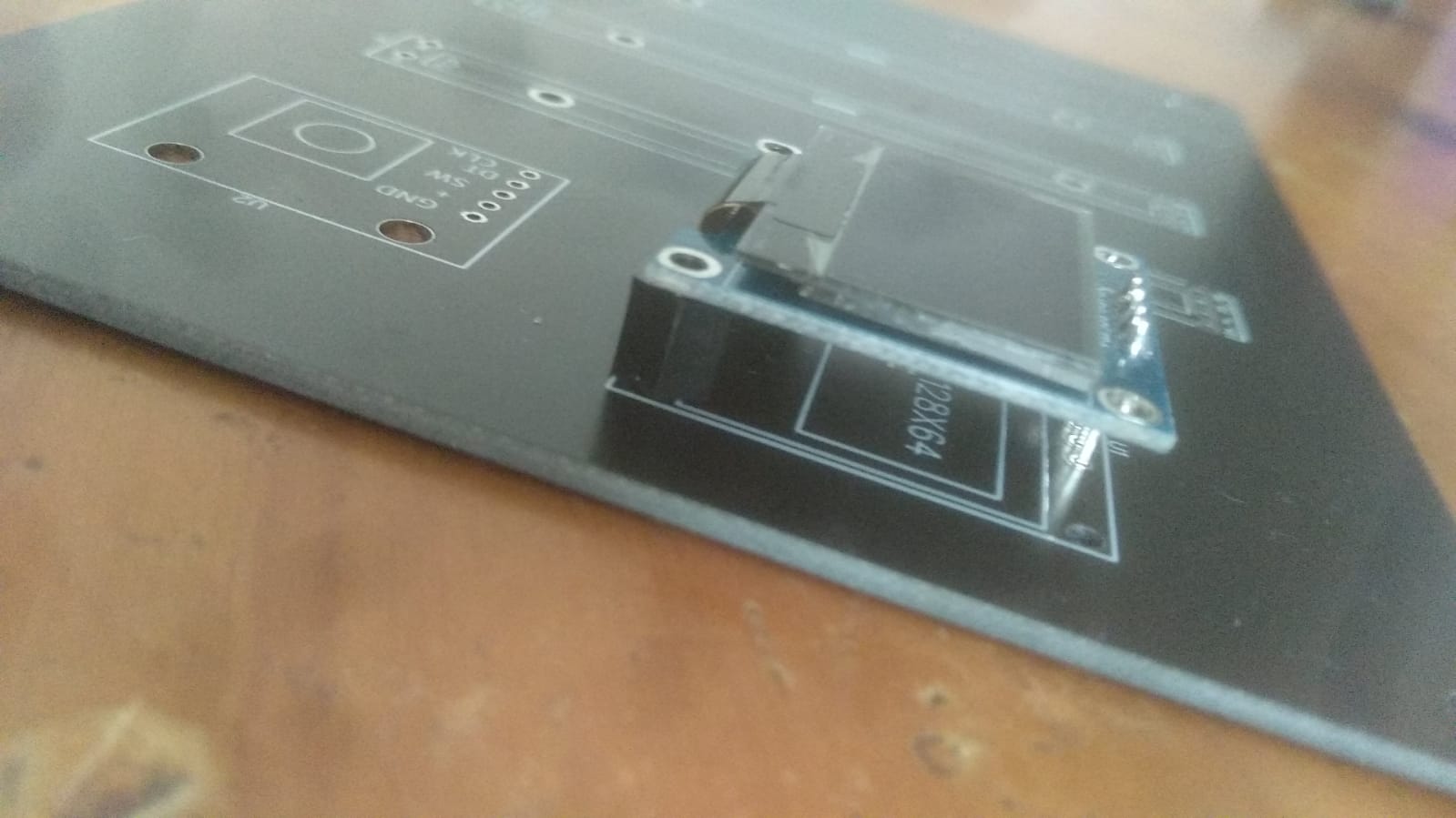
Maybe I'm misunderstanding what you mean, but isnt what you are describing, what I've already got going (in regards to the PCB)? If I understand correctly, I just need to remove the current header and add stand-offs to the 4 screw-holes and solder the OLED pins directly to the PCB, correct?

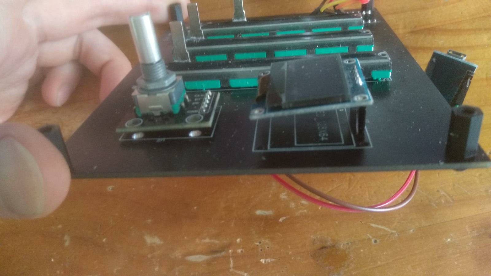
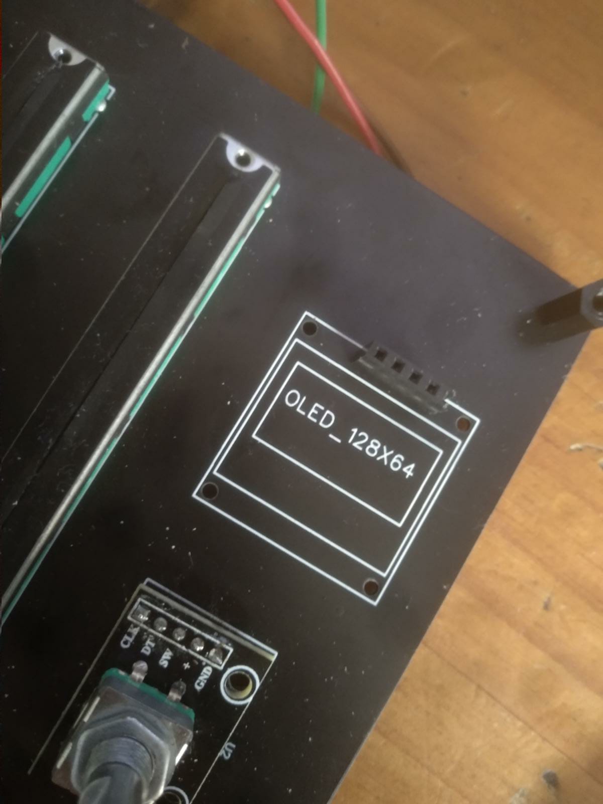
Basically like this, just with correct stand-offs (I dont dont currently have fitting ones on hand):


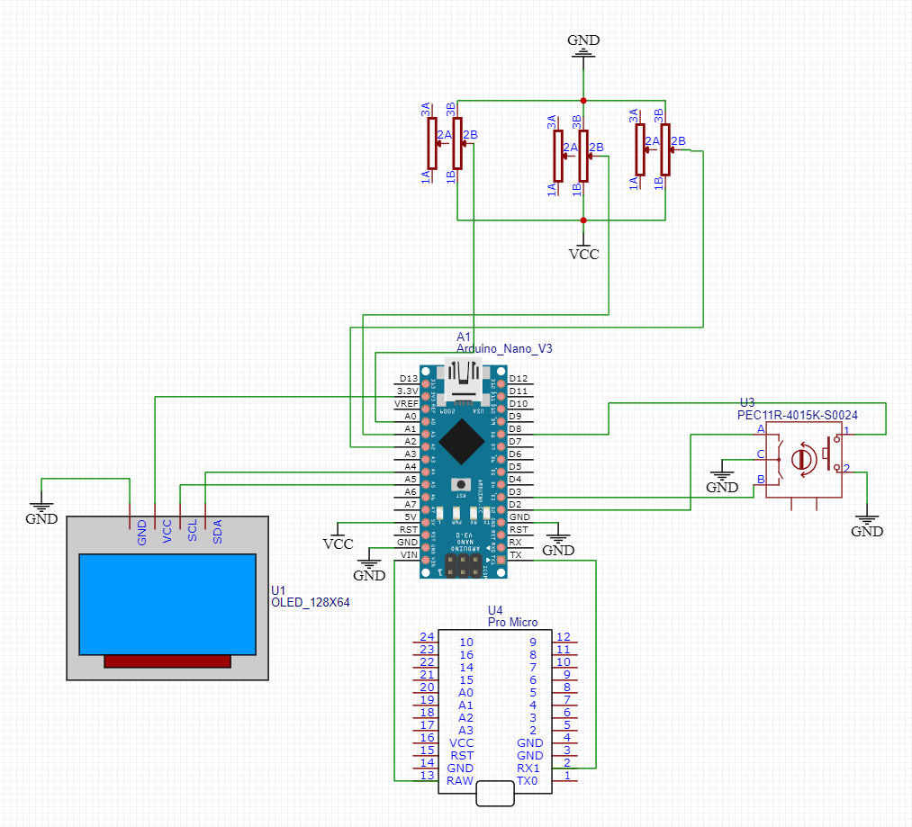
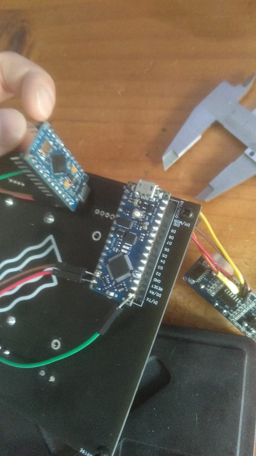
I was panning on soldering it onto the board, just like I did with the NanoEvery (in this case I added some headers so I can remove it for Testing purposes as I am still in development).

The ProMicro is currently only connected via some jumper wire (while I sort out the PCB design).

The Pro Micro is currently connected via the USB connector and delivers power to the NanoEvery via the RAW pin (AFAIK its some kind of direct-passthrough of USB power). Additionally I have the GRD and RX Pins connected (receiving MIDI data from NanoEvery).

Long-term I am hoping to redesign everything and have it working on a single chip, but that's something for for the future.
I'd also like to then replace the arduino board and mount the ATMega32U4 chip directly to the PCB instead of having the Arduino Daughter Boards on there. But that's something (again) for the future.

Instead of using headers, I suppose a proper DIP socket would be the nicer mounting option.

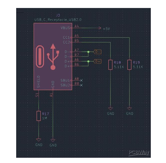
The reason I dont want to use the USB connector on the ProMicro is that the board is in the way (the usb connector is pretty much flush with the board). I want to manufactur a nice chassis and want the footpring to be as small as possible. Having only the USB connector (instead of the entire board+connector) gives me more flexibility on the placement of the USB connector, and the design of the chassis. Also, USB-C is the superior USB connector in every way, so if I add USB anyway, I want it to be the best type of USB connector.


EDIT: Is there a "best practice" when it comes to the layout of resistors and capacitors? I'm struggeling with the layout on the PCB. Looks very messy, and I cant seem to get the VCC connected to the Via (software doesnt seem to let me).

EDIT2: I found out there is an "Auto Route" option. If only I'd known that 6months ago when I did the first PCB :rofl:

AFAIK now all I need to do is get the USB-C connected :face_with_monocle:

I use a lot of these:

They look like what I need. Cheers LarryD!

Yes, absolutely right. I just didn't see the pattern under the OLED. You have already done the hard work.

:+1: FYI recent prices of the 32U chip have been high and the 4809 has been much cheaper.

With low frequency parts (the encoder will not be turning at 1000s of RPM, the layout is not critical.
I would just group each pin's components close to each other.

Are you using a ground plane (copper pour)? That is well worth doing, because it will simplify your layout,
In EasyEDA, you don't need to get a precise outline for copper pour. In the PCB layout, select the dashed rectangular tool from PCB tools palette. Select the bottom copper layer. Just draw an area larger than the PCB, and it will fill all the unused bottom layer with copper. A tip: the dashed lines you draw will be red even if you have selected the bottom layer. But as soon as you complete the polygon/rectangle, it will turn blue.
I will often do a copper pour on the top layer for VCC. Again, select the top copper layer and the dashed line tool.
If you do auto-route or move your traces, then jut re-pour the copper and everything will look right again.

Some other thoughts:

  • Make sure you rotate all your silk labels to be the right way up. Will look more professional :smile:
  • The labels should not be on pads
  • Don't forget to use the bottom silk layer for things like your board name, date, revision no, etc

It looks like its all coming together nicely. Hope you will show us your final result when you're all done!

That may be, but unfortunately it wont suffice. The NanoEvery actually uses the 4809, so unless I can port everything onto a single chip, Ill need that one too. The reason I need the 32U4 (the ProMicro or Leonardo) is because of its native USB support. Otherwise I would have had this project dont 6 months ago (only just finished the code and the serial connectivity between both boards) :smiley:

Yes, I just had it turned off so you could see the top and bottom tracks. This is what it currently looks like (Copper Layer for GRD, that's the usual way of doing it, right?).

I can show you a rendering of the current result, but I've recently considered redoing the whole design:
https://www.artstation.com/artwork/q9DlqN

Instead of the wooden frame with rounded corners, I'm thinking of doing something similar to the old MOOG synthesizers, where the whole thing is black sheet metal with the sides being flat wood. I'll need to do some design iterations, but the layout of the components won't change.

I'll definitely share the result when It's done, thanks so much again for the help.

Do you have any knowledge in regard to connecting USB-C? AFAIK the required pins are Vbus, D +, D-, GND, CC1 and CC2.

From my understanding:
VBUS -> VCC (5V)
GRD -> GRD
CC1 -> 5.11k resistor -> GRD
CC2 -> 5.11k resistor -> GRD
D+ -> ?
D- -> ?

can you confirm the above, and do you know what to connect D- and D+ with? Are those the RX/TX pins on the ProMicro or something completely differnet?

That looks fantastic!

The copper pour for the ground looks good too. I have used the top copper for V+ pour, and this has saved me some vias.

I will have to think a little bit about the USB.

Here is a schematic I found:

Take a look at it please. I think it is going to be very hard to do a direct wire.
As you can see, the USB D- and D+ go to the 32U D- and D+ via a resistor each. The diagram says 22 ohms, but I would double check that value.
It would be easy enough to add the resistors to your PCB. What I don't know is if the 32U D- and D+ pins are accessible and/or easy to hand solder to.

Thanks, I just stumbled across the schematic aswell. It doesnt seem like the pins 3, 4 on the 32U4 (D-, D+) are available on the Pinout of the ProMicro :confused:

Then again, my end-goal was to have the chips soldered onto the board directly...soo my thought process at the moment is that I can just skip the ProMicro and add the 32U4 chip onto the PCB now and add the NanoEvery manually. Eventually I could then have both chips soldered to the board.

The ProMicro only has 2 pins attached to the NanoEvery [Power and TX, (and GRD)] and would only need 2 pins connected to the USB-C connector (D+, D-), so it should (AFAICT) be rather easy to setup, or am I missing something?

Doing the NanoEvery would be a pain as I'll need a tonne of the pins, but this ProMicro replacement with the 32U4 should be somewhat of a plug-and-play?

Please correct me of my naivety has gotten the best of me again :sweat_smile:


Does anyone know what these holes in the PCB for the Potentiometers are for?

Are you supposed to bend the thicker pins under the potis to secure them to the PCB or whats the idea behind that? On my prototype I wasnt sure what they were for and actually soldered them to the PCB :rofl: Seeing that the potentiometers are solderd down (very securely) with 5 pins already, I'm not sure that the thick ones in the centre need to be soldered for security...right? I'm genuinly curious