First of all I must say that this solution that I will put here is definitive, BUT it is done with unconventional tools, such as an air soldering station, to remove the integrated circuit from the board, and a microscope to make the cutting and tracing work.
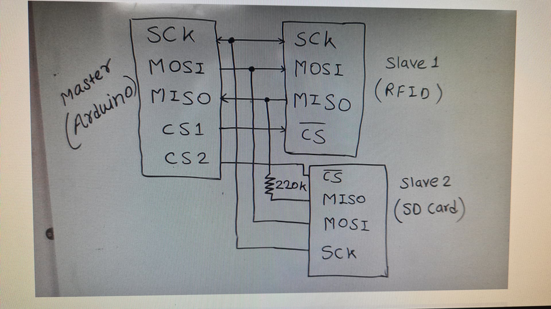
The SPI BUS has 4 wires, three of them goes from the MASTER (Arduino) to the SLAVEs (external SPI boards): MOSI (Master-Out to Slave-In, sends data from the Arduino to the slave boards), the clock signal, where the Ardunio controls the times of the signals, and the SS or slave selector, which chooses which of the SPI slaves it will work with. To keep in mind for this work, this signal activates the slave by a LOW signal, while if it is HIGH, the slave comes to disabled. And the fourth wire, MISO (Master-In Slave-Out), which goes from the SLAVEs to the MASTER (Arduino), carrying the signal with the data of all the slaves. If two or more of these signals (coming from two or more SPI devices connected to the SPI bus at the same time) are on the MISO BUS wire at the same time, they overlap, generating interference and invalid data.
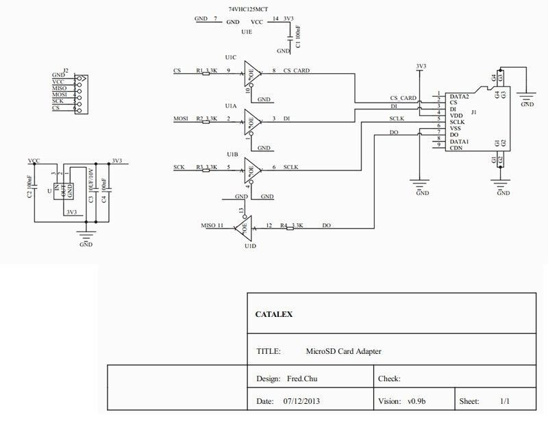
The SD card module uses a 74ABT125PW integrated circuit to control the four wires of the SPI bus. For this, it uses four line controllers with 3-state outputs: output in L or H same state of the input when the controller is LOW, and high impedance ("off", "no voltage") if the controller is HIGH, controlled by output enablers (OE pins), as if they were a transistor. In particular, these inputs enable the output by LOW signal, and not HIGH (like NPN transistors does). We can see in the module diagram, that these pins (OE, pins 1, 4, 10 and 13), are ALL grounded, so the enablers are ALWAYS enabling the four controllers. Enabling those that go from Master to Slave does not affect the operation of the SPI bus. But constantly enabling the MISO wire is a circuit design error, since the board would be constantly sending its information, even if it is not its turn (chosen by the SS). So, how to solve it? As the drivers of the integrated circuit are activated by LOW and what was said before about the SS signal (that it also enables by LOW signal), we are going to use the state of the SS pin as a driver enabler that activates or deactivates the MISO wire (pin 13) of the module. The SS wire enters through pin 8 and exits through pin 9, and can be connected to any of them, since being always active, the input signal will be the same as the output signal. For convenience of location and circuit, we will use the output, pin 9. So, the objective is to join them: that pin 9 sends its signal to pin 13.
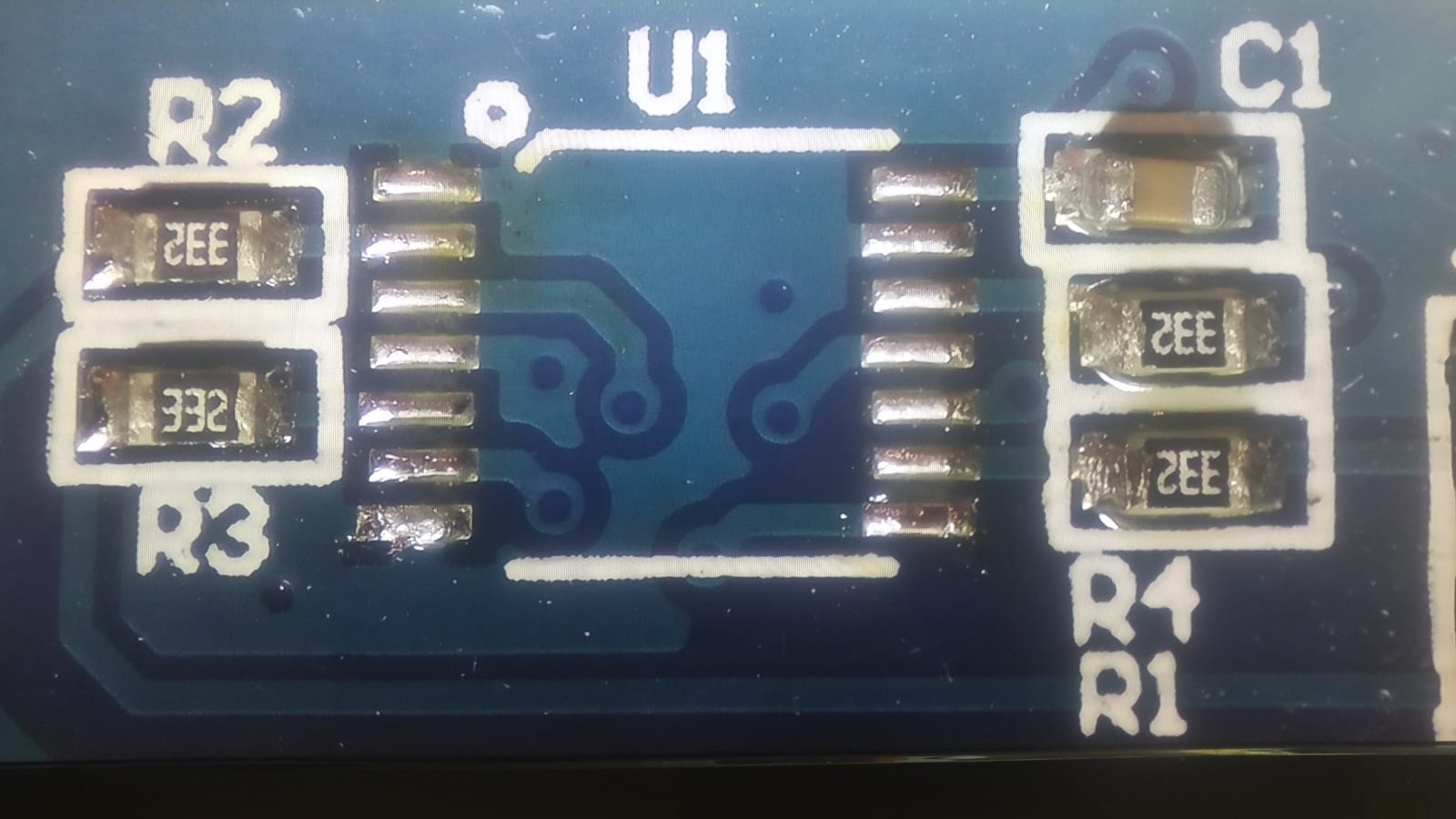
To start, we desolder the integrated circuit 74ABT125PW
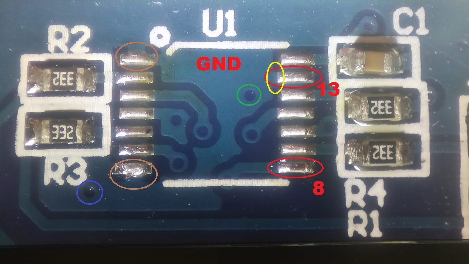
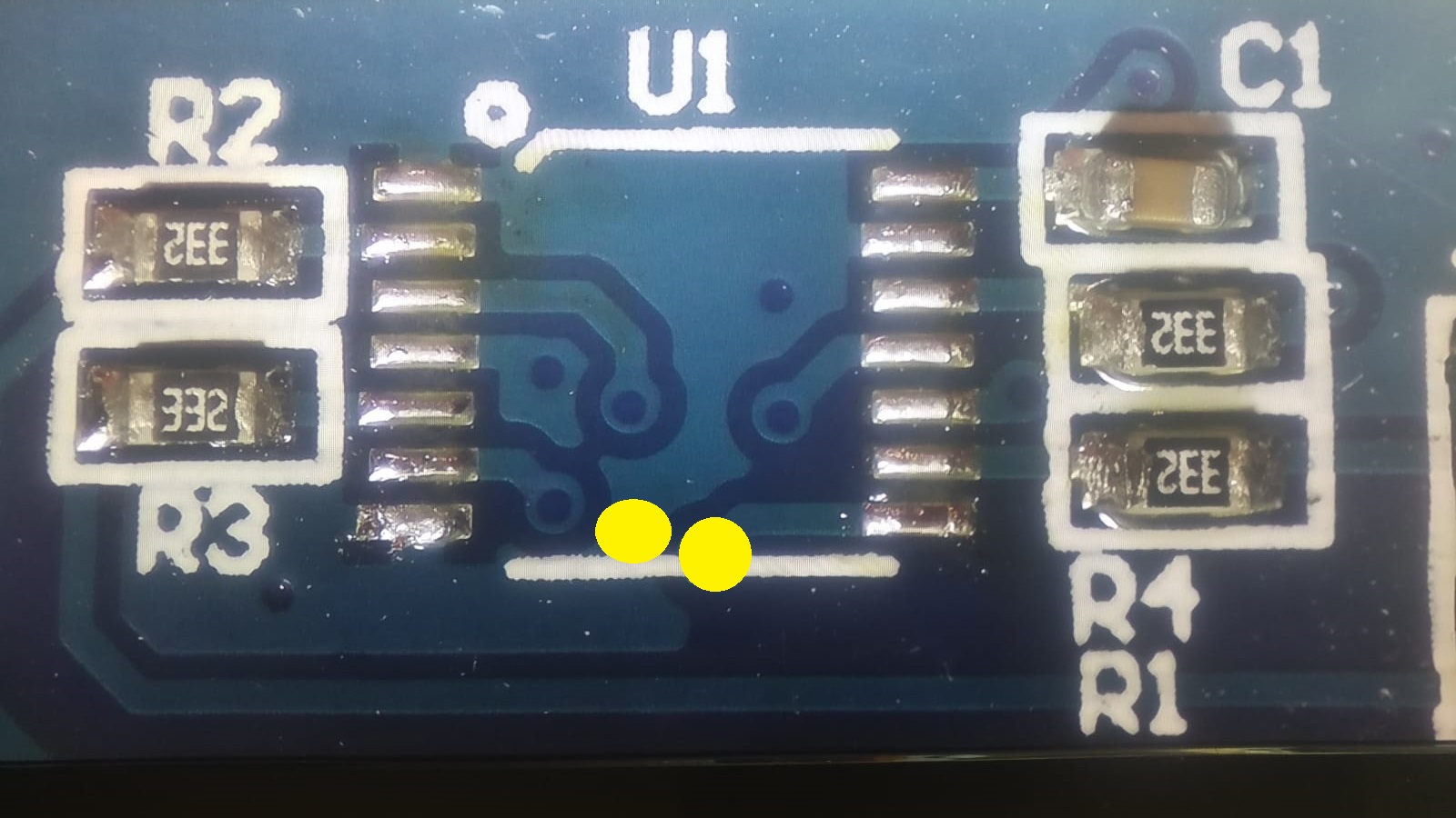
Here we have pins 13 and 8, which we must connect to each other.
As you can see in the yellow circle, pin 13 is connected to ground.
In the green circle there is a pass to the other side of the tile, where there is more mass, so at work we must leave it outside the line that we are going to try to do. If we remove it completely, there is no problem, since the masses will continue to be connected, for example in the same way in the blue circle. Anyway, after doing the new path, you can test continuity between pins 1 and 7 (in the brown circles) of the integrated circuit.
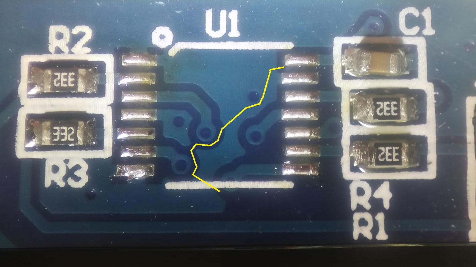
Once the path is done, we will scrape where the yellow circles are, until leaving the copper in sight. Then we will join the two tracks directly with tin (if you can't, put some wire on it)
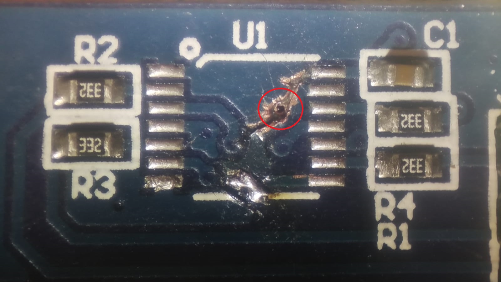
And here we've got it finished
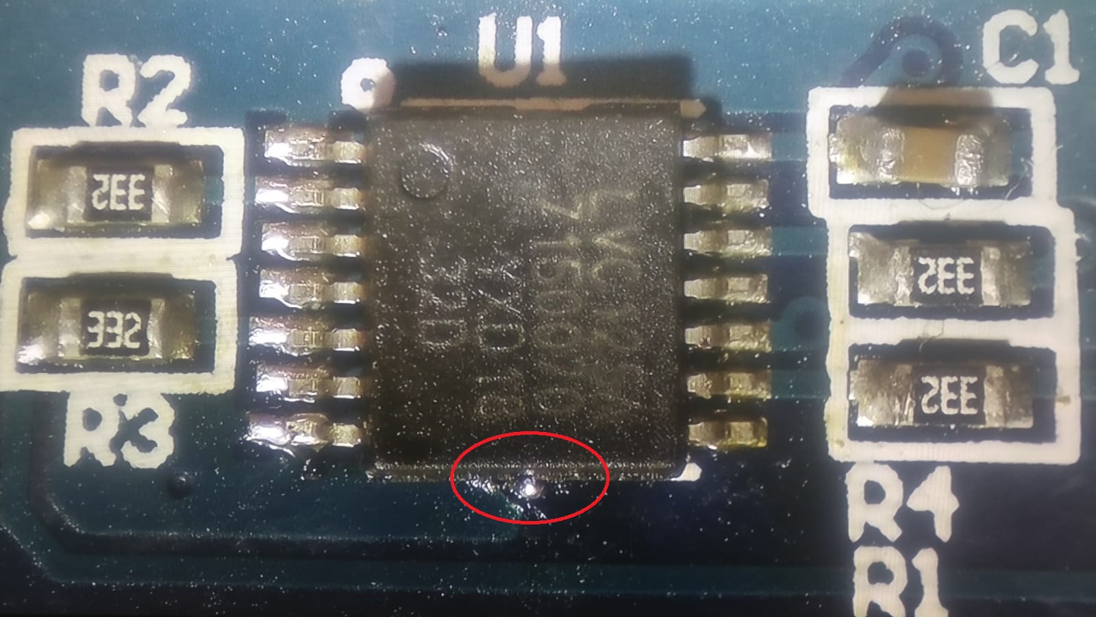
finally we solder the integrated circuit again
we can see how the tin sticks out a bit under the IC
And finally, since the problem was with RFID that works with 3V3, and that this module internally also works with 3V3, after lowering the 5V input with a 1117, I removed the regulator and joined the input with the exit pins. Just be carrefull, now the module MUST BE powered with 3V3 only
In my sketches I enable the board that I am going to use (setting them to LOW) and I disable the others (setting them to HIGH) every time I am going to use one of them, since I don't know if libraries do it internally.
Xakko