Project construction example and hints
If you are new to making projects, below is a process you might want to try.
Rather than using a prototyping PCB, we will build the following project on a copper clad PCB ‘mother board’.
After you decide what you want to make, draw a schematic of your design showing ‘all’ the components in your circuit.
There are many free PCB software packages for schematic design and PCB layout.
If your design uses a SMPS (switch mode power supply) always add a ‘Ferrite bead’ to snub switching spikes.
Construct your circuit on a solderless bread board to prove that the circuit works as expected.
Gather all parts and finalize their layout; make sure parts will fit in the project enclosure.
We will use some readymade components to simplify the following construction.
Components:
- Arduino Pro Mini
- SMPS (step up DC to DC converter)
- SMD MOSFET
- SMD 1206 resistors
- Ferrite bead
- SMD to THT “daughter boards”
- Kynar 30 AWG wire
- 24 AWG stranded wire for off board connections
- power switch
- IR LED
- power LED
- machined pin headers for the Pro Mini and SMPS PCBs
- one 3 AAA battery holder
- .06” single sided copper clad PCB called the ‘mother board’ (for mounting components)
- .03” single sided copper clad PCB (for manufacturing pads)
- enclosure/box
- heat shrink
Tools:
- drill press
- 1/10th inch prototyping PCB (referred herein as the ‘matrix drilling board’ template)
- metal hole punch OR metal shears
- ultraviolet glue
- PCB tinning solution
- 5-minute epoxy
- header pins for aligning pads to drilled holes
- 3 pinch clamps
- ‘D’ engraving bit (used to chamfer holes)
-
Make a paper copy of the 1:1 mirrored image of our ‘PCB pad layout’.
-
Tape the layout to the copper side of our ‘mother board’. Note: components that do not have their pins matching a hole location on our ‘matrix drilling board’ need to have those holes drilled free hand. These holes will be referred to as ‘major holes’.
-
On the paper image, center punch these ‘major holes’; discard the paper image.
-
Drill the ‘major holes’.
-
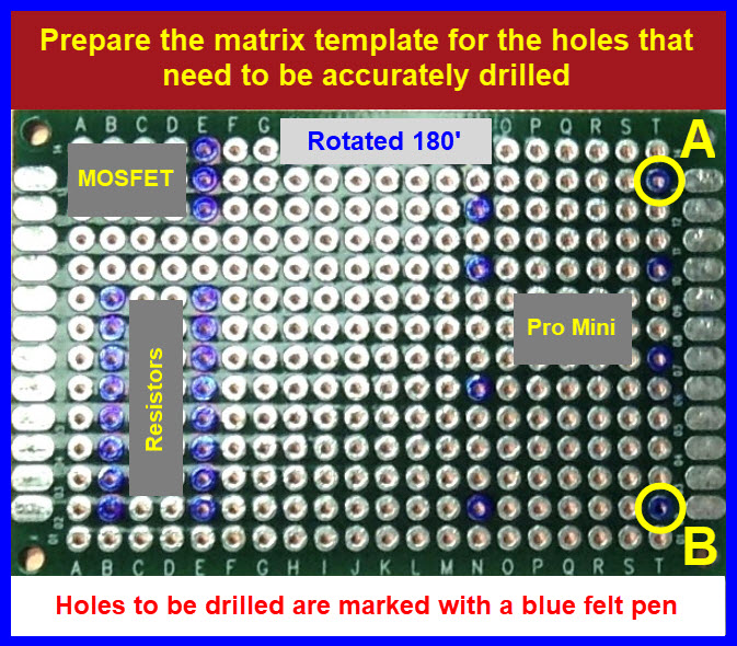
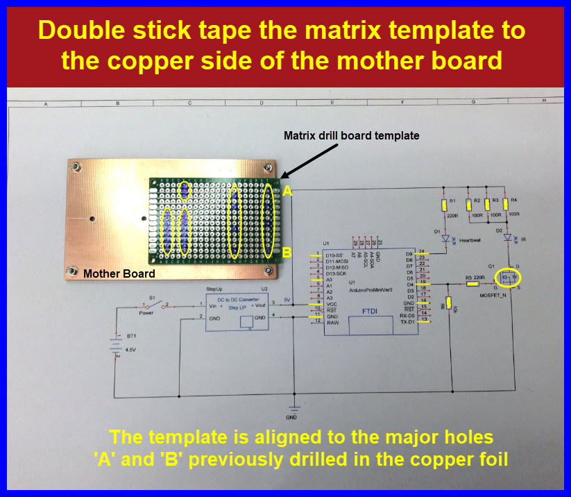
Align the ‘matrix drilling board’ to holes ‘A’ and ‘B’ as seen below.
-
Tape the ‘matrix drilling board’ to the ‘mother board’.
-
Use a blue felt pen to mark all pads that need matrix drilling.
Note: the drilling template allows for accurate drilling of matrix holes. -
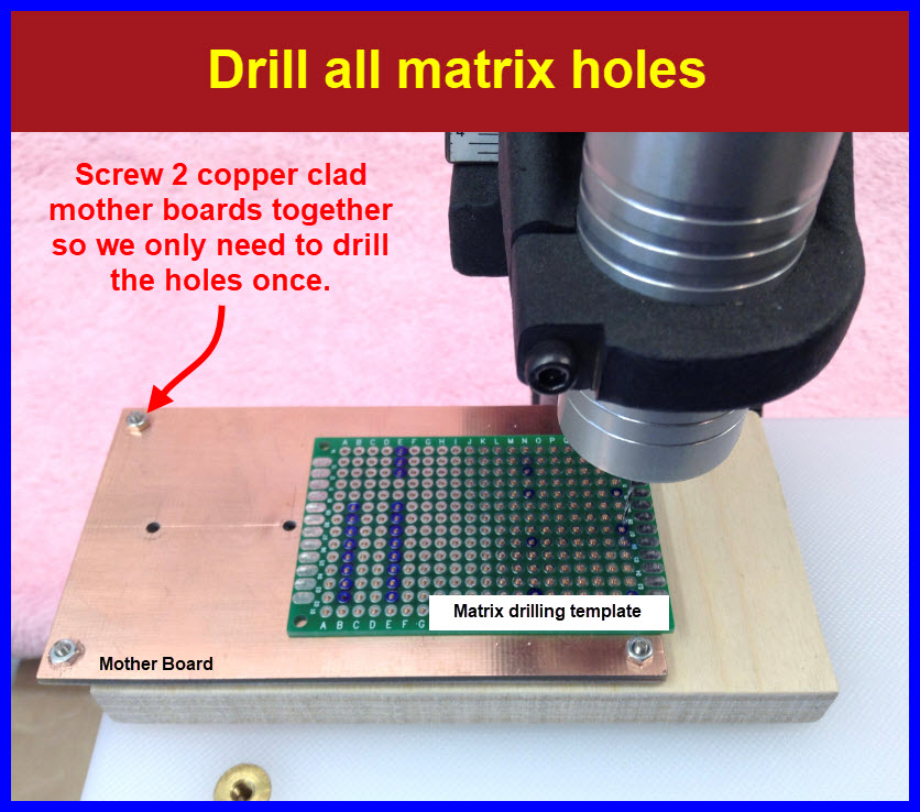
Drill all the blue matrix holes.
-
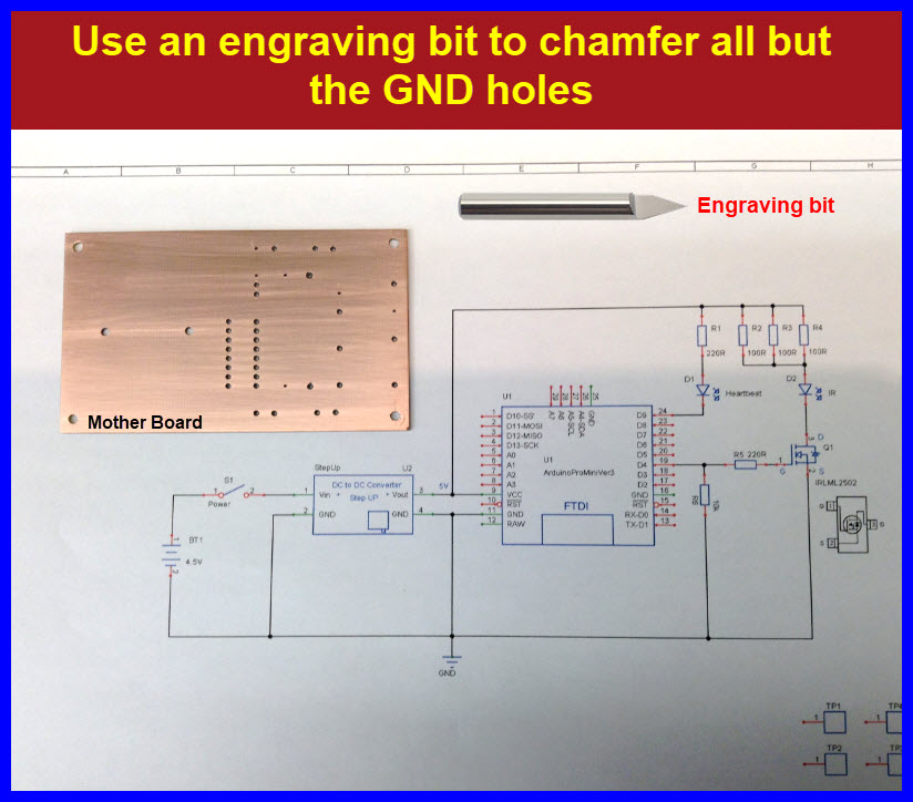
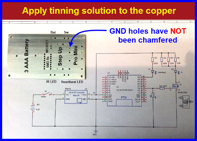
Use an engraving bit to chamfer all BUT the GND holes.
-
Submerse the drilled board in tinning solution.
-
Add machined pin headers to the Pro Mini and SMPS boards.
-
Fit these boards into the ‘mother board’ holes; solder all GND pins on these boards to copper foil.
-
Punch multiple pads from the .03” SS PCB material. (Alternatively, use a shear to cut square pads from the same material .)
-
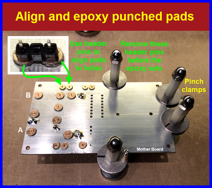
Align and epoxy these pads over the drilled holes, avoid getting glue inside the drilled holes.
You can use header pins to align the pads to the holes in the mother board. Remove these pins before the epoxy sets. -
Align with header pins and epoxy the SMD daughter cards onto the top surface of the mother board; remove the alignment pins before the epoxy dries.
-
Using the schematic as a reference, make a wiring map.
-
Solder 30 AWG Kynar wires as per the wiring map.
-
NOTE: for the daughter boards, the insulation of the Kynar wire ‘must’ go all the way through the mother board.
-
For strain relief purposes, add UV glue where off board wires leave the PCB.