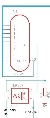
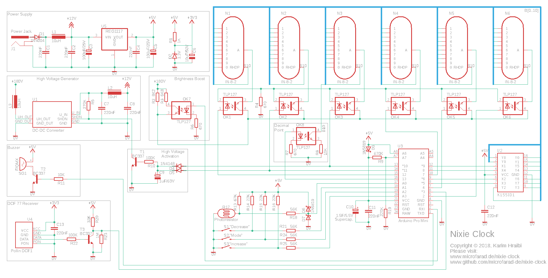
Unfortunately, I can't easily get a simulation model of this device (LTspice) to see what happens when it is switching this voltage and can't see how the base of the first transistor is biased etc., but can a user generally assume that if the datasheet of a photo darlington optocoupler is specified (normal operating parameters) for a Collector Emitter Voltage of X volts, it can switch X volts and this is independent of the connection topology emitter follower or common emitter ?
1- What's wrong with "the first transistor '
A- It's a an opto-coupler.
There is no 'first transistor'
It's an opto-coupler.
It's driven by a led.
"I can't really see what happens when it's switching this voltage"
What's to see . It's a transistor.
It turns on.
It's a switch (with a slight voltage drop)
Can you see what happens when you turn on a switch ?
2- "How is the base biased ?"
What kind of question is that ?
It's an opto- coupler.
There is no base.
What you're calling a base is a 5000V
photonic dialectric barrier.
It's not biased period.
It's either on or off.
Is that ALWAYS the case with opto- couplers ?
A- NO.
It's just happens to be the case here.
Why ?
A- Because the led is driven by a GPIO pin,
which I would hope you know is either on or off.
If the led were driven by a variable voltage
source then it would be possible to vary the
number of photons crossing the barrier and
therefore vary the 'bias' as it were of the transistor, resulting in less than 130V on the emitter.
Since it is either on or off there is 130V or no voltage on the emitter so the word 'bias' is not even applicable here unless you describe it as
'in saturation mode'
Nothing to see.
No 'bias'
No 'first transistor. ( it's a led)(driven by a GPIO pin)
Just the one transistor. (the darlington driver) No others.
No base (at least no physical one because it's
a photonic barrier)
You already have the datasheet.
Look up the collector emitter voltage drop when in saturation mode. It should be pretty small
so it might be 129.5V on the emitter.
OK @Raschemel, thanks for all that and a very entertaining style too. You did understand the the construction of the that particular optocoupler was a photo Darlington pair and the conventional model in the specification has a representation of a base (even though it is not externally exposed in that case). My reference to the first transistor, in case it is not clear, was to the first transistor in the Darlington pair facing the LED.
I'll simplify it a bit with another optocoupler (this time a single transistor design) which additionally exposes the base for optional external biasing. This one I can simulate in LTspice. I have 2 diagrams, one without external biasing on the base and one with some. In both cases, I am driving the internal LED hard. Without external biasing, I am losing about 8 volts over the optocoupler although I believe I am staying in specification for the device. With external biasing, I can eliminate the voltage drop. Hence may original question relating to the voltage which could be switched with such devices.
The conclusion I make from this and the comments received (thanks also to @Paul__B) is that if an Optocoupler does not provide an external base connection, the user can assume that it is capable of switching, without significant loss, the maximumum Collector-Emitter voltage specified (as long as everything is with in the normal specified operating parameters). In other words, the internal LED is capable of fully saturating the (output) transistor and the opto coupler functions equally on the high side or the low side.
You did understand the the construction of the that particular optocoupler was a photo Darlington pair and the conventional model in the specification has a representation of a base (even though it is not externally exposed in that case). My reference to the first transistor, in case it is not clear, was to the first transistor in the Darlington pair facing the LED.
Trust me . I know what a Darlington is, however, the 'first transistor' you refer to (the darlington driver)
IS the photo-transistor facing the photon barrier so everything I said still applies. The datasheet indicates
a 0.3 V drop.
You might find this a good read
When a transistor in a Darlington configuration with base-emitter resistance is incorporated into an Si chip, stray diode Di is put between the emitter and the collector in an equivalent manner. Owing to this, for VECO, the characteristics in the forward direction of the Di also appear; VECO is thus specified with a very low (0.3V) value. Through this Di element, a current flows between the emitter and the collector. The circuit must be designed so that the VECO value (0.3V) will not be exceeded.
In both cases, I am driving the internal LED hard. Without external biasing, I am losing about 8 volts over the optocoupler although I believe I am staying in specification for the device
You're only driving the led with 33mA. (SEE PAGE-6 of datasheet top right plot. Look at the collector
current difference between 30mA and 50 mA forward current )
Try changing the led resistor in the first simulation to 100 ohms for 50 mA.
OK. You were right about the LED resistor being too high. Assuming a forward voltage of 1.4V, the resistor should have been 72 ohms for 50mA which appears to cause the output transistor to saturate without external bias under these test conditions. I've revised the simulation:
OK. You were right about the LED resistor being too high.
Actually, it was just a SWAG (Scientific Wild Ass Guess).
I first looked at the max forward current spec, and then found the forward current vs collector current plot.
I actually was not thinking about the led forward voltage because it is not shown on your simulation so I
had no idea what it was. In reading your OP (OP has two noun meanings, when referring to the Original Poster and also when referring to the Original Post (the ONLY post in a thread that does NOT have
a Reply# assigned to it (because it is not a reply obviously). The OP is also the ONLY place the post title
can be permanently changed. Each poster replying can change the title in his specific replay but it only
changes it for that one reply , whereas the OP is the ONLY person who can change the post title in all
future replies and he can ONLY do that in the OP (Original Post). So, you can say the OP changed the title
in the OP. (which sounds funny but that's what it is) . So , for example, just for giggles, you could change
the post title in the OP to "Driving Darlington Opto led for Maximum Saturation"
(which , personally , I think would be far more informative since it a implicitly states your objective instead
of simply using the name of the device (as you have done) which does not say anything about your objective or reason for posting. As a general rule , since there is , at any given time, more than likely,
more than 100 years of experience (if you add up the cumulative working experience of all the members
following this topic (General Electronics). I , myself have 40 yrs. Grumpy Mike I think has 50, and one of the Pauls has 50 , so if just Grumpy Mike and myself replied to a post that's already 90 yrs, and if you
throw in Wawa , MarkT, LarryD, MorganS, JRemington, and a couple of others like Crossroads, your
probably up to about 250 - 300 years experience, so choosing a post title that says everything about
what your objective is can speed up your target acquisition exponentially because if they know exactly
what you are trying to do just by looking at the post title they can post the answer on their cell phone
while taking a crap. Problem solved.
I don't want to prolong this topic too much, but I have just come across this (APS1241/APS2241), which I am just mentioning because it is an exception to the models previously discussed in this thread. It is a low voltage opto-coupler which must share a common ground with the controlled circuit. It is available in two variants, one with an open drain output and one with a totem pole (push/pull) output.
I don't want to rai on your parade but the
whole point of having a 5000V dialectric
barrier is to ensure COMPLETE ISOLATION
between the interfacing systems because
replacing an entire MCU is much more
costly in parts and dowmtime than replacing
a blown optocoupler.
raschemmel:
I don't want to rai[n] on your parade but the
whole point of having a 5000V dialectric
barrier is to ensure COMPLETE ISOLATION
between the interfacing systems because
replacing an entire MCU is much more
costly in parts and dowmtime than replacing
a blown optocoupler.
Yes. The advantages of an opto coupler are crystal clear.
There is no connection implied between the grounds of the controlling circuit (the GPIO pin of the MCU, the opto coupler LED etc. ) and the controlled circuit on the isolated side. Unique about the (APS1241/APS2241) is that it must be on the LOW side sharing a common ground with the isolated application circuit. That was the sole reason I mentioned it.
I don't consider my parade "rained on" but neither have I much more energy to discuss the topic further.


