Hi all,
after quite a long time I have some latest results on my „little“ challenge – and I like to share. And I feel some duty in doing it because this thread has been in the Top 5 in the General Electronics category in this forum in 2022 ![]()
First, why it took some more time (despite the fact having, e.g., a job etc ...)?
As promised, I designed a PCB to get rid of stray inductances, and have some low impedance grounding network. It took some time as it has been my first one using KiCAD, and then ordering of parts of quite disturbed by adding parts to my BOM one day, and two days later there were sold out, so that I had to look for alternatives. Then, also, my first PCB with SMD, so I solder some test boards first...
I also did further investigation on Compensation Network 1 (or 3) in #63. It is actually a Zobel network, and so there where a guideline available in how to design. Despite, I turned out that parameters of it are not that critical as long it is there.
Furthermore, I was asking in another Forum for help – which triggered some further thoughts. And, finally, I was looking for better MOSFET with lower capacitances.
All ended up in a test circuit like below:

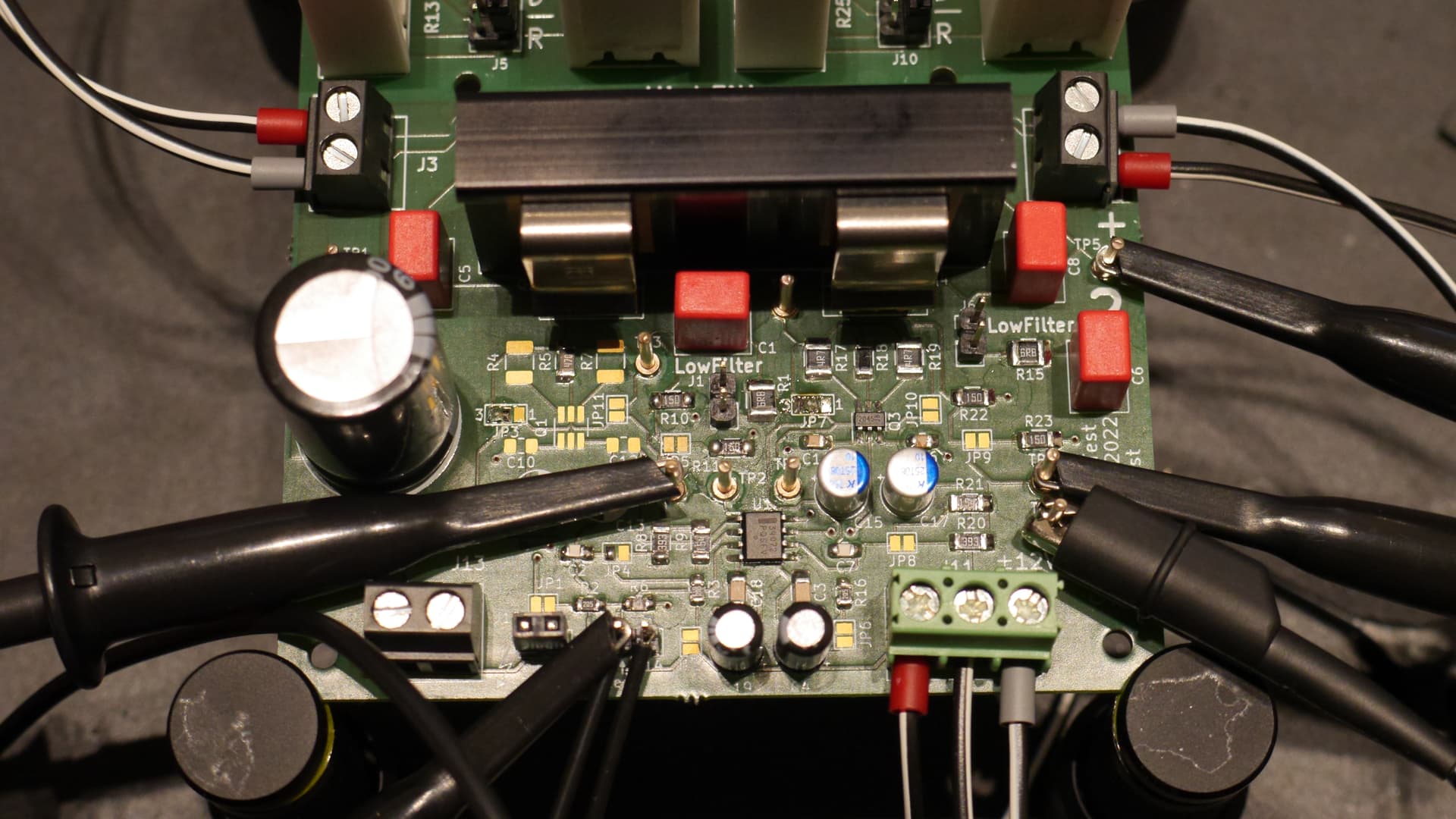
and corresponding PCB (bare, my first one!!).

What do you the in the circuit:
Same circuit two times. I build on my PCB two variants: One using the ZXTC2045E6 (Q3), one not populated. For sure, for the non-populated side (left in circuit), R5 has been choosen to be 47R, also C10-C13 where not used (in the following I only refer to left part of LED Current Control (Index 1))
Load can be simulated in five versions: for 12V as resitive load and as diode. Same for 40V. And, with LED spot under consideration. I began with low voltage to investigate, sure.
There is no direct connection between Source of Q2 and load. This is done via J3 and J4. Intention is to put long wires in between! I ended up to put here some Ethernet Cat 5e cable, which has an inductance of about 500nH/m, and of which I several meters here lying around.
See below one of my test setups (using the Cat 5e cables), including a close look on the assembled board. You may say it looks chaotic, wires all over the place – this is done on purpose, i.e. I didn't care (except looking for shorts).

Variant with Q3 has been dropped. Non-linearity caused by Q3 has been found to impose risk of instability.
Some measurements with (all use same scope parameters)
- JP1, JP2, JP5 and JP11 open
- JP4 closed
- JP3 connects Pin 1 and 2
- Yellow trace: TP4 (i.e. Current), shall follow the blue one.
- Purple trace: Pin 2 of J4, i.e. lower side of LED but the far end of the cable, AC-coupled
- Blue trace: input (J14, Pin 1)
- Green: TP1, i.e., like purple trace, lower side of LED but near end of the cable, AC-coupled
- corner frequency of C2 and R8/9 set to 220kHz
SDS00129: 0.5m cable, 1% duty cycle. All nice and stable!!

SDS00130: same as before, just showing that voltage across LED is changing not symmetrical (for whatever reason).

SDS00135: 15m cable. A difference between far and near end can be seen (purple and green differ from each other, oscillations on the far end. But current is looking good!

SDS00141: tried to maximize oscillations. Occurs at 0% - 100% step for load current for short pulses. Here for duty cycle of 0.12%, which is a 900ns on-pulse. But voltage at source of MOSFET looks well damped.

So, to summarize: it's working ![]()
![]()
![]() . Even with long cables!!
. Even with long cables!!
And, finally, what happens if the Zobel network is not in? See below for step 0%-50%, running just at 12VDC and Z-Diode as load and a duty cycle of 1.5%, while corner frequency just 150kHz: Quite a lot bad damped oscillations also at source of MOSFET and also current through shunt R10.

There were calculated using graph theory. Results were obtained by matrix calculus directly in frequency domain.
EDIT
And a picture of the spot I'm using when driven with lowest current (far below 1mA):

and highest current (around 130mA) with identical camera parameters
