I bought several MC6828 Priority Interrupt Controllers (PICs) and would like to use my Arduino Uno to test them. These are peripheral chips for Motorola's MC6800 and MC6809 CPUs.
I've built a test harness on breadboard and written code. At first I thought the chips were bogus (bought from Chinese seller) but I found the same behavior with another (bought from US seller) so think I've messed up my hardware setup.
Background
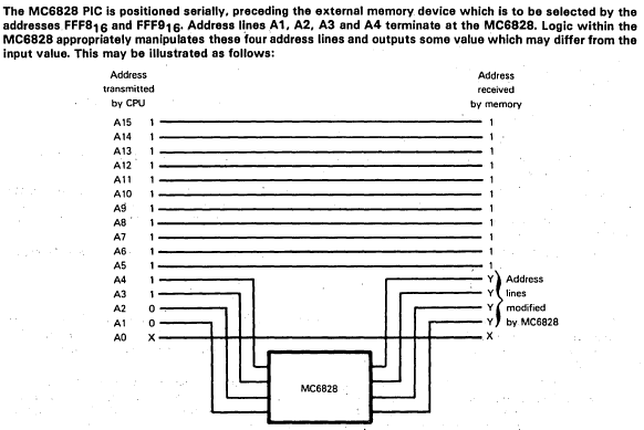
When the MC6800 CPU receives an interrupt signal (IRQ input pulled low) it requests the location of the interrupt service routine at memory locations $FFF8 and $FFF9. The 6828 can change the address requested depending on which of its eight input lines is pulled low.
It does this by sitting on four lines on the 16-bit address bus (A1-A4). During ordinary operation the 6828 passes the A1-A4 bits through to Z1-Z4. When an interrupt pulls one of its eight interrupt lines low the 6828 signals the CPU IRQ line and then sets Z1-Z4 so that execution jumps to an address that is specific to the incoming interrupt.
Test Hardware
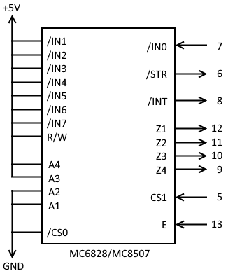
This high-level schematic illustrates where the 6828 sits in relation to the CPU and the "external memory device" (i.e. ROM).
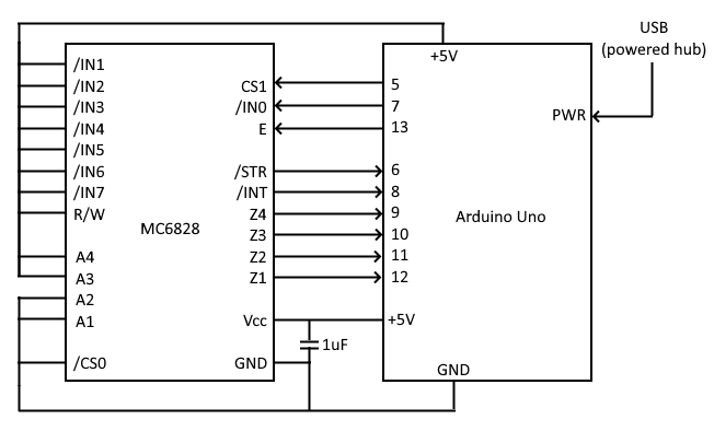
This abbreviated test harness schematic shows how I've configured the testing hardware. GND and +5V connect to the Uno. The Arduino controls the clock input E, chip select CS1, and IN0 (interrupt zero). It monitors the CPU interrupt INT, Z1-Z4, and the clock stretch output STR.
The 6828 datasheet defines a HIGH output as >= 2.4V (and the INT output is open collector) so pullups are activated on the Arduino input pins. LOW output is 0.5V.
Expected output on Z1-Z4 is b0010.
Algorithm:
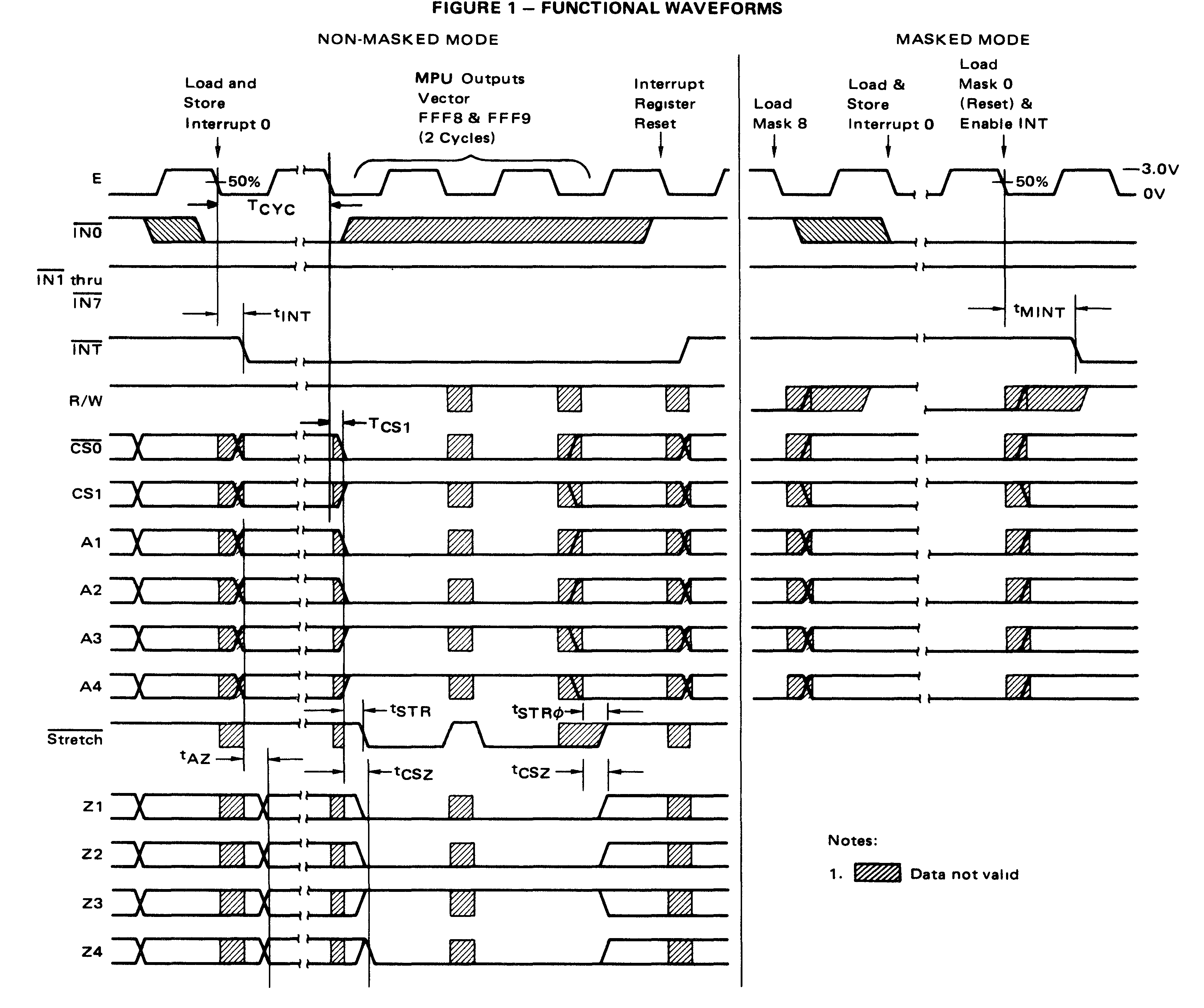
Here is the waveform diagram for the interrupt process (ignore the "Masked Mode section") as well as a functional flowchart (flowchart has an error: it says interrupt vectors go on A1-A4 when they actually go on Z1-Z4).

Here's my code:
/*
MC6828 Priority Interrupt Controller test program.
*/

// 6828 outputs
const int _6828_STR  =  6;  // inverted
const int _6828_INT  =  8;  // inverted
const int _6828_Z4   =  9;
const int _6828_Z3   = 10;
const int _6828_Z2   = 11;
const int _6828_Z1   = 12;
// 6828 inputs
const int _6828_E    = 13;
const int _6828_IN0  =  7;  // inverted
const int _6828_CS1  =  5;


void clockPulse(const int clock_pin) {
    digitalWrite(clock_pin, HIGH);
    delayMicroseconds(1);
    digitalWrite(clock_pin, LOW);
    delayMicroseconds(1);
}

void print6828PinData(const char* msg) {
    int intPin     = digitalRead(_6828_INT);
    int stretchPin = digitalRead(_6828_STR);
    int z4Pin      = digitalRead(_6828_Z4);
    int z3Pin      = digitalRead(_6828_Z3);
    int z2Pin      = digitalRead(_6828_Z2);
    int z1Pin      = digitalRead(_6828_Z1);

    Serial.print(msg);
    Serial.print(" : ");
    Serial.print("/INT: ");
    Serial.print(intPin);
    Serial.print(", /STRETCH: ");
    Serial.print(stretchPin);
    Serial.print(", Z4: ");
    Serial.print(z4Pin);
    Serial.print(", Z3: ");
    Serial.print(z3Pin);
    Serial.print(", Z2: ");
    Serial.print(z2Pin);
    Serial.print(", Z1: ");
    Serial.println(z1Pin);
}

void setup() {
    Serial.begin(9600);

    Serial.println("Initializing Arduino pins...");
    pinMode(_6828_INT,  INPUT_PULLUP);
    pinMode(_6828_STR,  INPUT_PULLUP);
    pinMode(_6828_Z4,   INPUT_PULLUP);
    pinMode(_6828_Z3,   INPUT_PULLUP);
    pinMode(_6828_Z2,   INPUT_PULLUP);
    pinMode(_6828_Z1,   INPUT_PULLUP);
    pinMode(_6828_E,    OUTPUT);
    pinMode(_6828_IN0,  OUTPUT);
    pinMode(_6828_CS1,  OUTPUT);

    digitalWrite(_6828_CS1, LOW);
    digitalWrite(_6828_IN0, HIGH);
    digitalWrite(_6828_E,   LOW);

}

void loop() {
    clockPulse(_6828_E);
    print6828PinData("Initial    ");

    // INj goes low
    digitalWrite(_6828_IN0, LOW);
    clockPulse(_6828_E);

    // PIC pulls IRQ low
    print6828PinData("Interrupt! ");
    clockPulse(_6828_E);

    // Processor starts interrupt routine
    // Processor puts FFF8 on address bus
    // Decoder enables PIC
    digitalWrite(_6828_CS1, HIGH);
    // Stretch goes low, slowing clock
    // PIC puts 1st interrupt vector on Z1-Z4 (0010)
    print6828PinData("Chip select");
    // Processor reads 1st translated address byte from ROM
    clockPulse(_6828_E);

    // Processor puts FFF9 on address bus
    // Stretch goes low, slowing clock
    // PIC puts 2nd interrupt vector on Z1-Z4
    print6828PinData("Vector2     ");
    // Processor reads 2nd translated address byte from ROM
    clockPulse(_6828_E);

    digitalWrite(_6828_CS1, LOW);
    digitalWrite(_6828_IN0, HIGH);
    print6828PinData("Clear      ");
    clockPulse(_6828_E);

    print6828PinData("Final      ");
}
[Edit: corrected subject; added expected Z1-Z4 output; moved images into text]