This thread is created being inspired by the following post of this thread to study the issue elaborately.
1. Referring to the IO section (Fig-1) of the ATmega328P MCU, it is known that after power up , DPin-2 (for example) appears as an input pin without internal pull-up resistor enabled. It happens so due to U2-Q (PORTD Register) = LOW though PUD = LOW and U1-Q (Data Direction Register for Port-D) = LOW.
LED1 is Off because G1 and Q1 are Off and there is no power source for R1-LED1 circuit.
2. Now if someone executes the following code, will KED1 be On or Off or half bright?
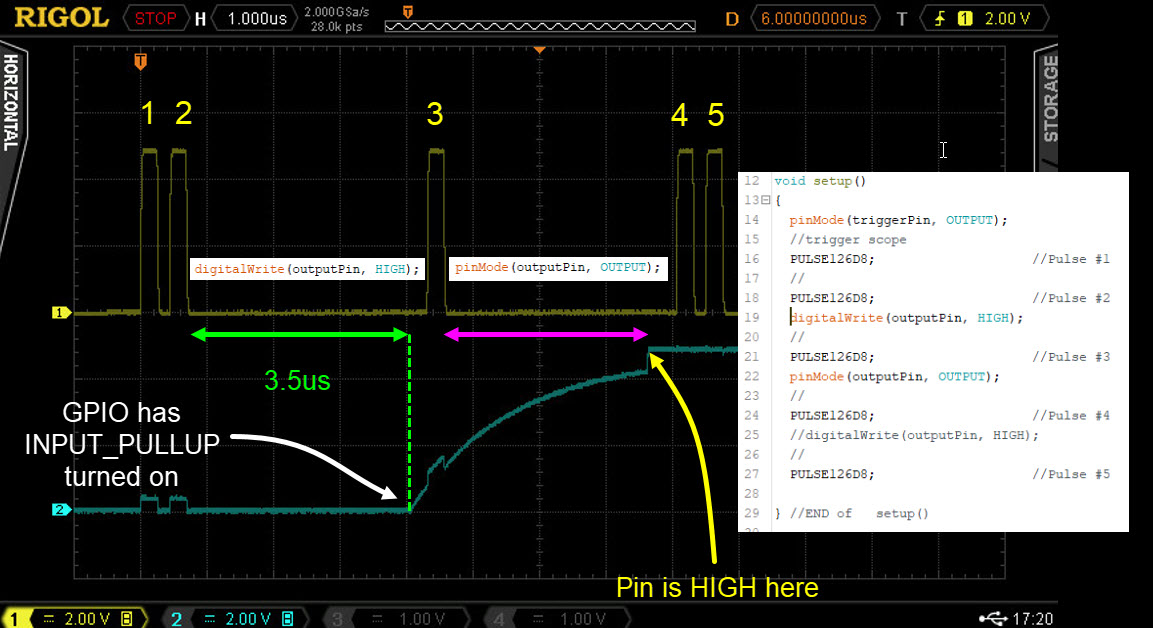
digitalWrite(2, HIGH);
pinMode(2, OUTPUT);
(1) From circuit analysis point of view --
G1 (power driver) is off because U1-Q = LOW;
G2 is On because U2-Q = HIGH due to the execution of digitalWrite(2, HIGH);
Q1 is On;
R1-LED1 circuit receives power from Vcc via Rip;
As a result: LED1 is half bright due to division of 5V across Rip and R1. The result is supported by experiment.
(2) To make LED1 fully bright, Q1 must be turned off to exclude Rip from the circuit. To do so, we must first execute pinMode(2, OUTPUT) and then execute digitalWrite(2, HIGH) to turn G1 (the power buffer) on. The result is supported by experiment.
3. Therefore, the order of execution --
pinMode(2, OUTPUT);
digitalWrite(2, HIGH);
is a requirement for the DPin-2 to work as an output pin.
In the linked topic the pin is not driving a LED. Remove the LED and place R1 between Vcc and pin. Hook up a logic analyser or oscilloscope and check what happens; if you don't have one you can (probably) use a second Arduino to measure.
During the reset the pin is in tri-state (INPUT) and can have any level. Because of (relocated) R1 it will however be HIGH.
When you switch to OUTPUT the output will go low; if pin 2 drives e.g a latch (that reacts on a rising edge) the latch will see a low level. Next you set the pin high and the connected circuit will see a high level indicating that the data on the latch's inputs needs to be latched.
If you first enable the internal pull-up (with digitalWrite) and next make the pin an output this will not happen.
The following test program is intended to demonstrate.
To make the LED only go from off to on, the order matters.
If you reverse the order, when you enable the internal pullup (digitalWrite the LED will be very gently driven. Then when you set the pin mode, the LED will be hard driven.
That pullup only period is enough to make some relay modules think they have been presented a HIGH state.
@GolamMostafa - if you aren't trolling, it looks like you did not even read what you quoted from elsewhere. You are invited to try this simple sketch
// https://wokwi.com/projects/452494236197117953

# define INTERVAL 777

void setup() {
 Serial.begin(115200);
 Serial.println("\nhi Mom!\n");
}

void loop() {
 Serial.println("STEP ONE");

 digitalWrite(2, HIGH);
 pinMode(3, OUTPUT);

 Serial.println("wrote 2 HIGH     set pin 3 OUTPUT");
 Serial.println("");

 delay(INTERVAL);

 Serial.println("STEP TWO");

 digitalWrite(3, HIGH);
 pinMode(2, OUTPUT);

 Serial.println("wrote 3 HIGH     set pin 2 OUTPUT");
 Serial.println("");

 delay(INTERVAL);

 pinMode(2, INPUT);
 pinMode(3, INPUT);

 Serial.println("reset 2 and 3 (INPUT mode)");

 Serial.println("\nWanna see that again? Pay attention!\n");

 delay(3 * INTERVAL);
}
In post #1, I have explained the theory of IO operation referring to the ATmega328P MCU.
The point I want to make is this: if you execute digitalWrite(DPin, HIGH) without first executing pinMode(DPin, OUTPUT), and then claim that the pin is HIGH at the output, that HIGH is fictitious. It is not a real output HIGH, because it is not driven from the PORT register through the output (power) buffer. The 1/2HIGH is coming from Vcc through the voltage divider composed of Rip and R1 (Fig-1 of #1).
It is your perception that I have quoted my text/saying from somewhere else! I have shown the reason why there apperas a fictitious HIGH at the output pin without first executing the pinMode(DPin, OUTPUT).
Since you have time to waste on this well-understood issue, why not drag in the UNO R4, the Arduino board in question from the thread you quoted but did not read closely?
With good faith and intention, you encouraged me to open a new topic to explore further questions. You have maintained your sanctity; however, someone else has acted otherwise.
Fig-1 of post #1 and the follow-up experiment demonstrate that if pinMode(2, OUTPUT) is not called upon before digitalWrite(2, HIGH), DPin-2 does not deliver a true VOH; instead, it produces a fictitious HIGH which makes LED1 (Fig-1 of post #1) appear half-bright.
Fig-1 clearly says the about the source of this fictitious HIGH. In order to get true HIGH/VOH from DPin-2, one must execute pinMode(2, OUTPUT) first.
Exactly--that is what is happening. As a result, Rip comes into the picture, and when one measures the open-circuit voltage at DPin-2, it reads 5 V and is mistakenly taken as VOH. This is a false HIGH, as evidenced in Fig-1 and also by the fact that when a load is connected (the R1–LED1 circuit of Fig-1 in post #1), the voltage collapses almost instantly (theoretically nearing to (5/(35k + 2.2k) * 2.2k) V).
If something does not work in theory, it will never work in practice.
Fig-1 of post #1 does not support the idea of making a DPin to function as a true output pin without first configuring its direction as output after power-up.
A programmer writes code to activate the hardware; therefore, the code should be aligned (one-to-one correspondance) with the hardware.
low activated relays would cycle once during power up..
/*
our relays are low triggered.
set the pin high before config pin to input.
avoids relays chattering on power up.
*/

  for (int i=0;i<numRelays;i++)
  {
   digitalWrite(relayPins[i],HIGH);
   pinMode(relayPins[i], OUTPUT);
  }