Hi everyone, I just made an account so this is my first post. I have a project where I'm using an ATtiny85 to control a 24V LED strip and 24V computer fan separately. I'm trying to learn but this getting is over my head now and would love some help.
It looks like using 2 mosfets is the best way but since I'm using PWM for the LED strip (for dimming) I was told I need to use a gate driver. The mosfets I originally had were 30V but was also told that I should go higher than 30V to be safe against motor kickback from the fans even though I do have a flyback diode in place.
Trying to keep this board about 35mmx60mm but if that's too small then I can go bigger. Lastly, I'm having JLCPCB make these so I'd love to find something in the LCSC library.
These are the two mosfets I originally chose for no reason other than they seemed to fit the bill at the time (the first one linked is in the schematic). You're more than welcome to let me know what else in my schematic is bad, I'm really new at this.
I think it will work fine. I’m assuming the ATtiny85 is running at 5V and that its ground is connected to the power ground. I also assume C3 and C4 are across the PWM outputs. I’d recommend not using them, as they could cause excessive current drain through the MOSFET when turning on. Some of the part numbers in the schematic are for sockets rather than MOSFETs. You did a good job with the bypass capacitors.
For reliable operation, make sure the 24V supply cannot exceed 30V under any fault condition; otherwise, your regulator and MOSFETs could be damaged. You might also consider using two capacitors on both the input and output of the regulator. If one fails, the system won’t be affected.
Thanks for the reply, I just updated the main post with the new schematic that I did maybe 10 days ago. That I'm sure changes things. Also, this board is coming from JLCPCB today! So I'll report back after I test it and see if anything goes up in smoke!
Appreciate the reply, I just updated the main post with the new schematic that I did maybe 10 days ago. That I'm sure changes things. Also, this board is coming from JLCPCB today! So I'll report back after I test it and see if anything goes up in smoke!
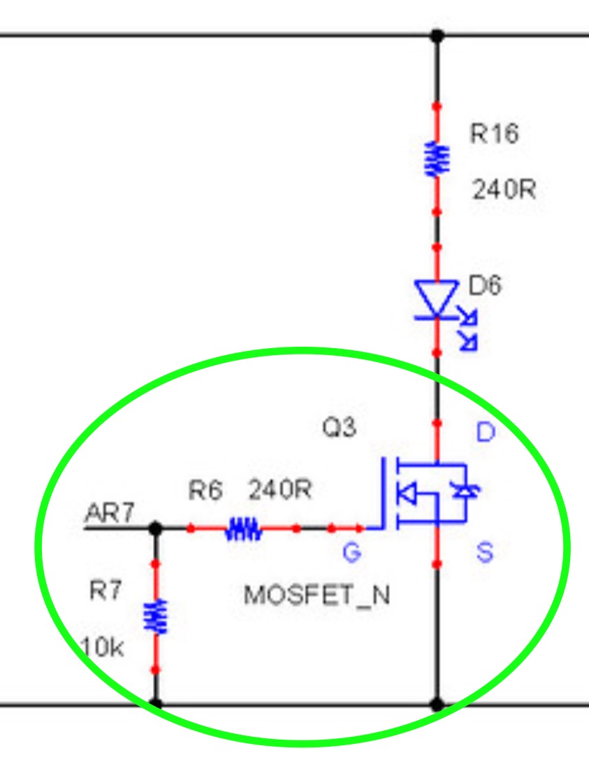
Thanks Larry, I'm pretty new to this but what it looks like is that the pull down resistor connecting the gate and source should be after the gate resistor. Is that what you're referring to? As you may have seen I updated the post with the latest schematic. I did these edits before you replied though so my layout is essentially the same. Everything I was reading was describing the pull down resistor being placed closer to the mosfet than the gate resistor.
The 10k pull down resistor is there for the Arduino pin, not for the FET.
It keeps the pin firmly grounded during boot, when the pin is still an input.
Leo..