You are missing a few things
Have a look at this schematic
thank you
if I need 3.3 V for my temperature sensor, do I need another regulator ?
and if so, do I connect it to the regulated side of the 5v regulator ?
Yes.
You will also need level translators to go from 5V to 3.3V for the I2C bus.
To keep things simple, you may want to consider a different temperature sensor (5V).
ok thank you so much for you time
A 5volt regulator with 5volt input?
A 3.3volt temp sensor?
Why not power both the MCU and sensor with 3.3volt.
So a 3.3volt volt regulator and an 8Mhz crystal.
No level shifter.
Or run the MCU on it's internal clock (no crystal).
Leo..
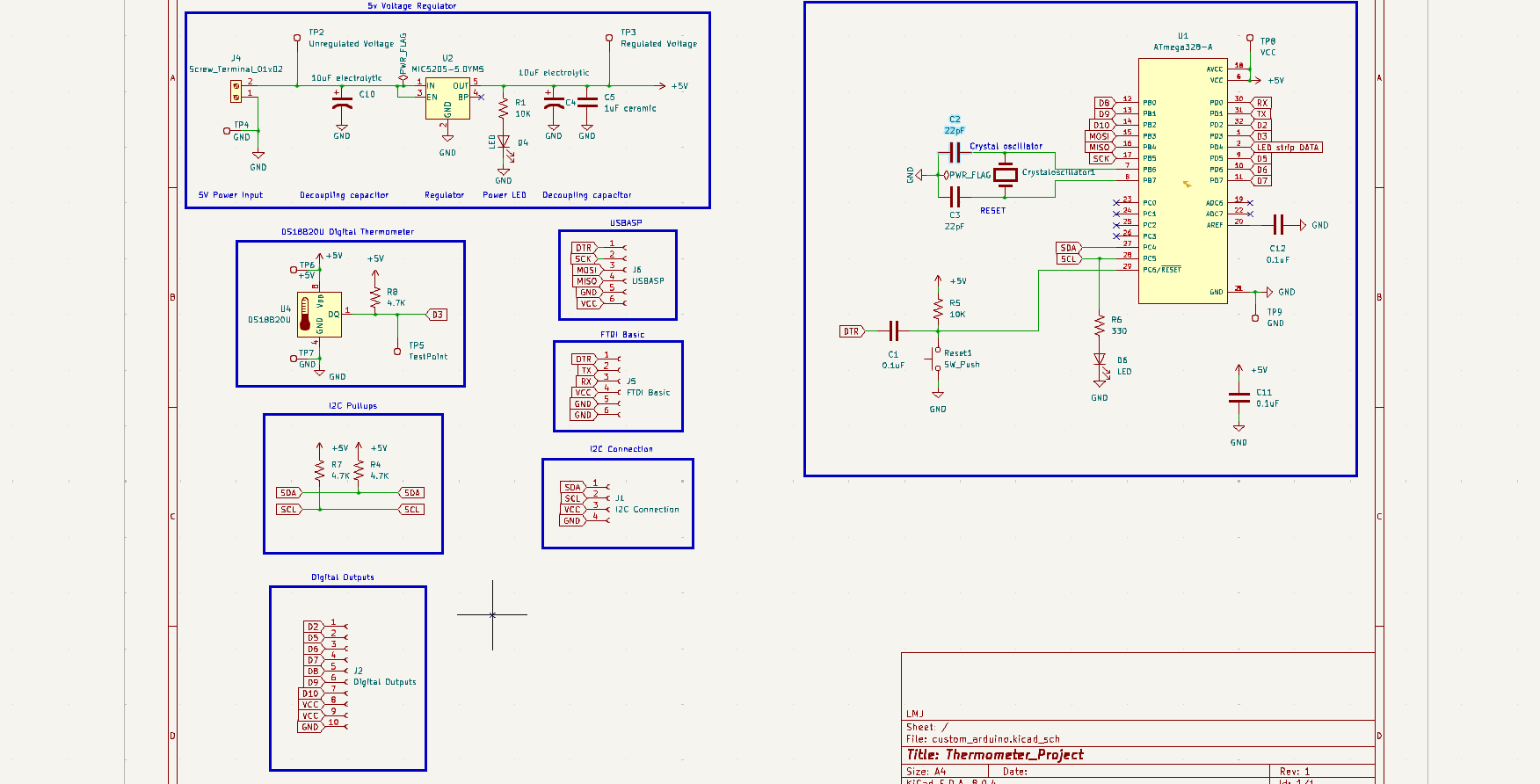

I believe C4 and C10 have to be tantalum not electrolytic
Did you intend to put an LED to ground on the I2C clock line? I'm not sure how this may affect the operation of the I2C bus.
Thanks for the catch. That was supposed to go onto SCK
Tantalum is electrolytic. And no, they don't have to be. In fact, I'd not recommend tantalum unless there's a very compelling reason to use them.
For 10uF at this voltage I'd just use smd ceramics.
You could put a single 47u or so aluminum electrolytic on the power input.
I'd move the indicator led to a different pin so it's not connected to either of the I2C lines. It's not very useful to have it there (can't use it if you're using I2C at the same time) and it may actually interfere by pulling down the pin to an undefined intermediate level if the pin is allowed to float high (note that I2C lines are never pulled high hard, they're only allowed to float up through a fairly weak pull-up).
@lmjiscool, do not crosspost. Threads merged.
Same difference.
I2C will not work if SCL or SDA lines are pulled LOW with a LED/resistor.
Still wondering why you use a regulator to convert 5volt into 5volt.
Or is that 5volt input label there to confuse us.
Leo..
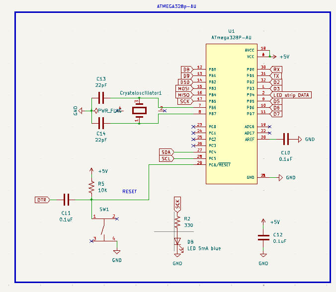
Will you be creating another schematic to post here?
Thanks too all of you for the great help. I really appreciate it  yes I will post my final schematic again for you guys to double check thank you



I think your power traces are a little thin, and it is bigger than required.
-
Place the GND pour on the bottom of the board, remove it from the top of the board.
An x-ray view is useless, show the bottom view, no x-ray. -
The traces do appear too thin. Your VIAs look small too.
-
What is the voltage going into the regulator ?
-
Put a series 470R resistor in the LEDstripDATA trace

5V input and 5V output ?
