I'm modifying a circuit design to use the ATMega328P-PU as a standalone chip instead of the Nano I've been using. Thank God, KiCAD is awesome and I have the MCU on a separate sheet where I can show simply the portion I'm working on.
I spent a lot of time reading about the various connections and there is some back-n-forth on whether or not AREF should be connected or not, as well as how to connect AVcc.
The datasheet does not state, that I found, whether AREF should be connected if it is unused. I believe the AREF can be selected to be used via fuses/registers and, if so, I intend to turn that off and use Vcc as the reference voltage.
The datasheet does state that AVcc should be connected via a low-pass filter to Vcc if it is used, seemingly leaving it unnecessary to use the low-pass filter if the ADC isn't to be used. This is the biggest area of uncertainty I have, the AVcc connection. I don't intend to use the ADC but I would like to have this design be robust so that I can use it for other projects where I may want the ADC. For high (whatever that means...kilo, mega, giga?) frequencies I found information about using a ferrite bead but that was deemed inappropriate by one commenter for low (again, what is "low"?) frequencies. That commenter then suggested using a RC low-pass filter but mentioned the voltage variation limitation between Vcc and AVcc (0.3v claimed). Ugh, I'm out of my league. Nothing I'm working on, or likely to work on, is super critical, so maybe this is overkill; but I don't know, so I'm asking.
Notes: the component in KiCAD doesn't have a pin 22 yet it shows up on the PCB needing to be connected to GND and it is. Also, the crystal is 16Mhz and its datasheet shows "Load Capacitance" of 20pf. I got confused when reading (too much) about that; whether that's the external capacitance needed or if there needs to be consideration for stray capacitance. Out of my league...again. Final note: I intend to program the MCU with an Arduino as Programmer, I will have no provision for ISP.
While this is a very simplistic setup, I have some concerns as mentioned; I'd like to ask for thoughts and input on this, please.
I have never used the lowpass (RC) filter on the AVCC pin, but just connect it to VCC. I think you did just fine and even gave it a separate decoupling cap.
AREF is a pin where you can provide a different (lower) reference voltage than VCC. When you activate that with Analogreference() function, the ADC will then measure from 0 - AREF instead of 0 - VCC.
If you connect AREF to VCC you make that feature no longer usable. If I were you I would break out AREF to a pad or pin, so in the future you could use it if you find a purpose for it.
On the PCB's I design, I use the leftover empty space on my boards to just break out as many pins as possible, without making the board bigger, just to be able to connect something to it in the future. More than once I was able to repurpose a previously designed PCB for something different. Especially when I had given the I2C pins a header.
This is very bad practice but Kicad put 22 under pin 8 and hidden it. So when you connect ground to pin 8 it also connects to pin 22
whether that's the external capacitance needed or if there needs to be consideration for stray capacitance.
It is not the capacitor you put on the PCB
so maybe this is overkill
No it is not.
You obviously have much to learn. Spend some time on the Microchip website reading the app notes for the 328 and ones for circuit design in general. I think you will find answers to all your questions.
Search for AVR042. A lot of good information in that appnote.
You probably don't need the crystal and 2x caps. Almost all projects will run just fine at 8MHz using the internal oscillator. It's very rare to find a project where 8MHz is too slow but 16MHz is fast enough. Generally 8MHz is enough, or 16MHz is also too slow!
The other reason for using a crystal is because it's timing is more accurate and changes less with voltage and temperature. This may be important for things like serial communications at certain baud rates. But again, for most projects, it's not a problem to use the internal oscillator.
Agree with the others, connect the RST pin to 5V with a 10K, not directly, and add a PCB pin or something so you can externally reset for programming or an external reset button.
Will you use a 28-pin ATMEGA328 in a socket? If so, you can remove it for programming.
totally agree. @hcb007 if you have "unused" pins - at least add a pinheader, you might "reuse" your boards for future projects. Also consider some additional VCC/GND headers.
Thank you for the reply. Understood re ranges for the ADC. You make a very good point about breaking out pins to pads "just in case" (and the AREF). As a matter of fact, I happen to have two PCB designs which I'm moving past and which will have extremely limited value...but had I left pads for pins.... I got excited, had them made, now condensing into one board. Live-n-learn.
Initial programming with a ZIF socket, board, and Arduino as Programmer. I had a PICKit3 (I never used and which died in a fire last year) which is the general concept: bare chip, burn a BIN/HEX, remove from programmer, install. I will use a socket to mount this, if I need to reprogram it then I'll pull it out. This is to be put into duplicates of a (sort of) tested design. The test device is a Nano.
Understood, thank you. Programming is intended to be done prior to installing the ATMega328P and it will be installed in a socket in case it needs to be removed to reprogram.
I edited the symbol. Yes, hidden under pin 8. Not hidden any longer. I don't have that symbol in my library, none of my DIP symbols for this chip show pin 22. Now that I know it's hidden I can at least edit the symbol and make it visible. It was already connected but having it more-clearly represented is better.
Got that app note. Thank you, that's got good info.
Thank you, Paul. The reasons for the crystal are twofold: 1) keeping things the same, the clock frequency/timing from the development board, a Nano, to the duplicates, and 2) I read that it can affect serial communications. I have two I2C devices I'm using currently and, as I'm already putting a lot on my plate, I didn't want to chase down another rabbit hole of "how does this affect that and how do I deal with it". But you are right, for what I'm doing, anyway, 8Mhz would be fine. It's really for continuity/similarity with between development and deployment.
Yes, each source which I have read about using a crystal has stated that the crystal is more consistent. Consistent inputs of "this is better" is good enough for me to do it. If that cold text reads as being rude, I don't intend that.
I had looked at the Uno and Nano schematics but had just read the 10k and 1k, respectively, resistors as pullups for the reset button. I will add a 10k to the reset pin.
I'll say something stupid here so you can correct me: why do I need the reset button if I'm not using it for programming? If it's for occasional lockups, I would think that's a development opportunity.
Yes, the chip will be in a socket expressly for removal to reprogram. I have a test setup which has been running for about 2 weeks at this time. It's functioning properly. That code will get put onto new chips to then be put into the field (literally...it's a ranch). Once it's deployed I don't anticipate the need to make any changes. Combine that with the rural setting and ISP isn't one of my design concerns; toting my laptop across fields...yeah, no. I can burn another chip and swap it in the field. That it's in a socket is testament to my understanding that I may think it won't need changes...but Life gets a vote, too.
Thank you, GolamMostafa...that was helpful. If I've read that correctly:
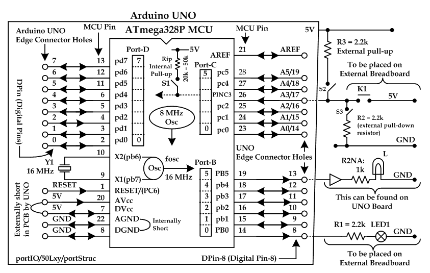
pin 22 is a separate ground for the ADC. In this diagram it's labeled as AGND, the first time I've seen that labeled as such.
if K3 is open, AVcc wouldn't be connected to anything.
with K3 and K1 closed, AVcc is tied to AREF and Vref. I read further that, if K3 and K1 are closed and AREF is connected to a lower voltage, then current from AVcc could back flow onto AREF.
My takeaways for my application are these:
connect AVcc to Vcc (if K3 and K1 are open it hurts nothing but if they're closed it's connected to an appropriate voltage)
while not shown here, I see no harm in decoupling AVcc near the input and will do so near the chip unless there's a good reason not to
connect AREF to Vcc (I don't anticipate needing the ADC and have no lower voltages in play)
decouple AREF as shown, also near the chip.
I read somewhere that decoupling caps are better-placed near or at the pins. Having no good reason to deviate from that, I will have the caps close to the pins.
I've saved that image with my other ATMega328 docs. Thank you again, that was very helpful.
Noiasca, yes, I agree. Totally on-board with that idea about the "unused" pins. Darned good idea on Vcc/GND headers. As a matter of fact, if I'd used both of those ideas on the PCBs I have in-hand, they'd actually be useful for other projects, just as you say. Worse, I had to scab onto a Vcc point on one of the boards as well as an Arduino pin because of "feature creep"...if I'd had "unused pins", Vcc and GND pins....
Okay, I read you on the ISP. And...back to the recurring theme of "put it there just in case".
Per the ArduinoNano30Schematic.pdf file I have, it's just the 6-pin dual row header I see on the Nano, not a large footprint to add.
Good catch...those should already have tags on them like so many other pins. I have a schematic with a Nano. I copied the schematic and removed the Nano and added the ATMega328 to another sheet because it's symbol is larger than the Nano and was sitting on connections/wires. I bungled something...those connections aren't where they are supposed to be in my schematic, I must have accidently deleted them. That's a goof on my part.
Yes, I see. I looked more closely at the Nano schematic and they connected AREF to ground through a 0.1uF cap. My thoughts are to make it more idiot-proof and connect both AVcc and AREF to Vcc so that if the registers aren't set correctly the Vref still sees what I would expect; Vcc. It doesn't seem it would harm anything to do so.
Yes, the registers should be set correctly and checked. But, I have been known to make mistakes...from time to time (daily).