Oh I think I may have interpreted the original schematic a bit incorrectly. I think now the C5 might make more sense with the modification I just made
One thing I don't understand is the reason for one of the capacitors being polarized when the rest are not. from the original schematic I mean
All you had to do, is move R3,R4 and you wouldn't have those horrible lines crossing on top of an IC. Your polarized cap is backwards. If it's a tantalum, it will appear to work for a while, then it will overheat and explode. Ask me how I know.
It's shown as polarized, because non-polarized caps of that capacity were not widely available until very recently.
yeah i know ill need to clean up the schematic I just want to make sure everything is wired up correctly first.
OH are you saying I can replace that part with a 10u non polarized capacitor then. such as this one.
CL05A106MQ5NUNC | Samsung Electro-Mechanics | Multilayer Ceramic Capacitors MLCC - SMD/SMT | JLCPCB
Cart before horse. "making sure" becomes a more reliable process, the neater and more readable the documentation is.
You may or may not decide to replace the polarized cap with an MLCC. You didn't say what you are currently using or why. Is it just because the Leonardo has one?
@anon57585045 Ive been using the original schematic as a base for what I want to do, (which is nothing complex circuitry wise I believe)
I want to make a pcb for a gamepad so ill basically only be adding buttons after im done recreating the basic schematic. For the buttons I plan to use the MCUs internal pull up resistors which I think for what im doing will probably work just fine.
If I didn't ask before, have you proto'd the entire system on an actual Leonardo?
No not yet. I have an Arduino Leonardo in my possession but I’m waiting for my delivery of cables and buttons and a breadboard to arrive in the mail so I can start testing/programming.
I just figured I could at least try to make the barebones schematic in the mean time.
I’ll probably be using one of the following xinput libraries for the programming though.
I also have a 3d printer which I plan to use to make an enclosure/controller shell but that will come more towards the end of course.
alright I took some time to try and clean up the schematic a bit. I imagine I can probably still do better but here it is.
Great, thanks! It seems to me like the +5V wiring has some peculiarities. You have the bypass caps in series with the power supply rather than in parallel. So the IC won't get any DC power. Actually, GND is connected directly to +5V.
It’s shorted isn’t it? At the moment the circuit will pass straight to ground after the fuse. But you’re saying even if I remove that ground that the way my capacitors set up I’ll still have a problem with getting power to the IC?
I’ve just been following the original schematic that I found and posted about and I know I’ve gotten everything right except for the part we are currently discussing as it was a bit confusing for me to understand from the original schematic.
I don't know. How do you intend to fix it? Just do your best and repost the updated schematic.
@anon57585045 ok, after doing a bit of searching online and checking the data sheet a bit etc . . . I think what I have now might be correct. I'm certain its closer to something correct vs the mistake I had before.
I can't vouch for the USB-C because I haven't played with those yet. But I don't see anything wrong with that schematic.
If you've never laid out a PCB before, that is whole new game.
Yeah it'll be a puzzle to lay this out on a pcb but that will be more of a test of skill in geometry and general placement.
I checked several sources for the USB-C.
What I have there is a USB-C USB 2.0 setup. Only thing different was needing to add a 5.1k resistor to each CC pin for it to work apparently.
Thats from wikipedia but I found a few other sources online that confirm what I've done is supposedly correct.
I compared it with a board I have with USB-C, it's the same circuit. So you should be good to go. Honestly, though, I only gave everything a "morning coffee once over".
no problem, I got a second opinion on the kicad discord and they said it looked ok as well.
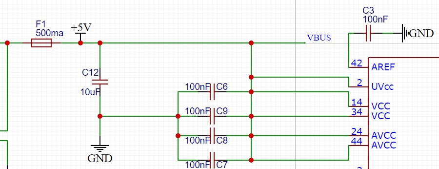
The only thing im wondering now is if I even really need that extra cap on the VBUS line though. I think it might be a pointless component in the circuit the way it is. (and that all my caps are mlcc)
For that, consult the IC data sheet. Or, sometimes that is parcelled out in an application note.
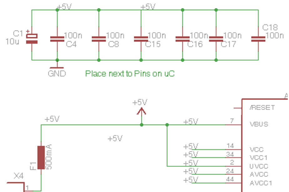
the IC datasheet indicates each vcc should be decoupled but that uvcc and vbus can share that 10uf capacitor so I've simplified it a bit to reflect this information.
Seems reasonable. Realize that the "decoupling each" Vcc means physically close to the pin, and grounded to a low impedance common such as a huge ground plane. Physical layout matters! AVcc is sometimes also decoupled with an inductor in addition to the bypass cap.
absolutely, and luckily the pins are all already close to one another. Ill probably only have some trouble with the placement of UVcc/VBUS/Ground.
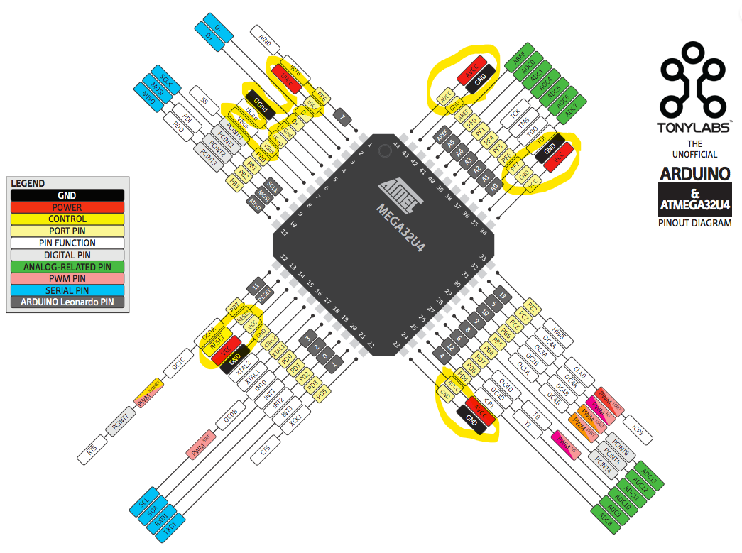
Even the Ucap, Aref and XTALS are close to ground pins (I guess the hardware engineers took all these things into consideration with the design)
Il'l more than likely have all my components placed on the top of the pcb and that way I Can make the bottom part into a giant filled zone for ground minus of course any via traces ill likely have to place for some of the routing.
I imagine that should work, ill have to do a bit more searching about that avcc inductor thing your talking about though everything I had come across so far online didn't seem to mention or have any inductors for the avccs.