Architecture of LX6 Processor and the Organization of Dual-core 30-pin ESP32S Board

Based on the following five diagrams, I have few questions that are given below:


Figure-1: Architecture of LX6 Processor


Figure-2: System architecture/structure from Espressif document


Figure-3: Schematic of ESP32


Figure-4: Dual-core 30-pin ESP32S Board

Figure-5: Functional Block Diagram of ESP32

My questions are:
1. Is the Flash Memory (U3) of Fig-3 marked as External Memory in Fig-2?
2. Is FreeRTOS firmware pre-installed in "Instruction ROM Memory" of Fig-1? Which core it is -- Core0 or Core1?

3. From where I can have the Pin Diagram along with signal signatures for the LX6 Processor

4. In Fig-5, UART is a peripheral which can be owned either by Core0/Task0 or Core1/Task1 (Fig-6). Then, eight IO lines (for byte transfer) must be emerging from each Core to a central hub/UART_Controller to route them to the UART for onward transfer to the OutputBox of the Serial Monitor. Does this make sense?


Figure-6:

Wouldn't it be more convenient for you to make your inquiry in the Espressif forum?

Regards

Thank you for referring me to the appropriate Forum. Can I post in this thread whatever answer I get from the ESP Forum?

I guess there is no problem, it just seemed to me that that forum would be more interesting because it is for these processors

It has been important for me to know the mapping of the LX6's hardware with that of the additional hardware of ESP32 imposed by Espressif in order to understand better programming using FreeRTOS.

I have already registered with Espressif Forum and have made a post. Now, waiting to read the responses which for sure will appear in this thread.

This is the answer I have received from ESPRESSIF Forum in response to my Q4. of post #1.

Note that the APB is pretty similar to any other multi-master bus, such as all those chips that support DMA to peripherals. The bus controller is in charge of which "host" can access which which "client", typically stalling all but one host if there are simultaneous access attempts to the same bus. It doesn't matter than one potential "host" is a CPU.

Somewhat fancier bus controllers (ie "bus matrix") can support multiple concurrent accesses as long as they don't conflict; for example a CPU could access code from flash memory at the same time a DMA controller is transferring data from RAM to a peripheral.

ARM chips usually have multiple bus controllers that vary in speed, and are part of the ARM intellectual property. There's an AHB high speed bus matrix that usually connects to RAM and Flash and perhaps some high-speed peripherals, an APB lower-speed peripheral bus. A SAMD2x processor has an AHB, three APBs, and an IOBUS. The IOBus allows some peripherals to be accessed in a single CPU cycles, while the more complex buses can take several cycles.

1. Is the Flash Memory (U3) of Fig-3 marked as External Memory in Fig-2?

I would assume so. The ESP32 doesn't have any internal flash.

2. Is FreeRTOS firmware pre-installed in "Instruction ROM Memory" of Fig-1? Which core it is -- Core0 or Core1?

I think FreeRTOS is in the code you load into flash (judging by the libraries and code that are used during the build process), and the ROM contains only the proprietary radio code (Hmm. Maybe more than that. Apparently there is even a tinyBasic interpreter!) ROM is accessible from either CPU (Section 1.3.2.1 of the Technical Reference Manual)

You have provided much more elaborate information than the ESPRESSIF Forum. However, (at the moment) I would like to be more specific to 30-pin ESP32 Board. Based on your opinion and the opinion of ESPRESSIF, my understanding is:

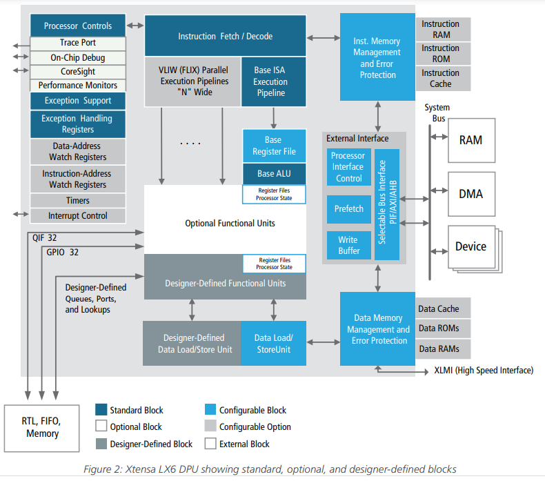
1. Ref to Fig-1 of post #1, each LX6 Core contains:
(1) Instruction Memory Block containing RAM, ROM, and Cache. Any idea about their capacities in bytes?

(2) Data Memory Block containing RAM, ROM, and Cache. Any idea about their capacities in bytes?

(3) I am interested to see the pin diagram of this LX6 Processor (Dataplane Processing Unit DPU) and the Technical Reference Manual.

2. This is the pin diagram (Fig-1, Section-5 of this post) for the 48-pin ESP32 Chip of Espressif, which contains:
(1) 2 pieces of LX6 processor -- is it correct?
(2) (a) 440 KiB ROM Memory, 520 KIB SRAM, 8 KIB RTC Fast Memory, and 8 KiB RTC Slow Memory as per Sec-1.3.2.1 of Tech Ref Manual -- is it correct?

(b) Are these memories together marked as "Embedded Memory in Fig-2 of post #1?
(c) Are they connected with both LX6 Cores by a "Memory Bus" other than APB/AHB/IOBus?

(3) Fig-2 of post #1 shows "Cache" -- does it exist within the ESP32 Chip? There is no mention of it in Sec-1.3.2.1 of Tech Ref Manual.
(4) Is Flash Memory (U3 of Fig-3 of post #1) a separate chip and it exists outside the hood of ESP32 Chip?

3. Are there APB (Advanced Peripheral Bus), AHB (Advanced High Performance Peripheral Bus), and IOBus (Input/Out Bus) in the ESP32 System? Is Flash Memory (U3 of Fig-3 of post #1) seen as a peripheral device?

4. With regards to the storage of RTOS and Sketch:
ESPRESSIF Forums has said in response to my query:
"FreeRTOS (plus every other part of the system: heap implementation, C library, peripheral drivers, network stacks, etc) is compiled along with your application and linked into the application binary. Application binary is stored in Flash. Parts of the application are copied into the internal RAM ("Instruction RAM" and "Data RAM" blocks of Fig.1 of Post #1) on boot, including some parts of FreeRTOS."

5.


Figure-1: Pin diagram of ESP32 chip

6.

If the "Bus Controller (a piece of hardware)" takes care of allocating resources avoiding deadlock/conflict, then why do we need software components like mutex and semaphore as is found in the following Arduino sketch (prepared consulting FreeRTOS manual and ChatGPT and tested) that shares common UART0 Port of ESP32 between Task0/Core0 and Task1/Core1?

//#include "freertos/FreeRTOS.h"  //inclusion is optional
//#include "freertos/task.h"
#include "driver/uart.h"   //this header file must be included

#define UART_PORT UART_NUM_0
#define BAUD_RATE 115200
#define BUFFER_SIZE 128

// Define the mutex handle
SemaphoreHandle_t uartMutex;

void setup()
{
  // Initialize the UART
  uart_config_t uartConfig =
  {
    .baud_rate = BAUD_RATE,
    .data_bits = UART_DATA_8_BITS,
    .parity = UART_PARITY_DISABLE,
    .stop_bits = UART_STOP_BITS_1,
    .flow_ctrl = UART_HW_FLOWCTRL_DISABLE
  };

  uart_param_config(UART_PORT, &uartConfig);
  uart_driver_install(UART_PORT, 256, 0, 0, NULL, 0);

  // Create the mutex
  uartMutex = xSemaphoreCreateMutex();

  // Create tasks for both cores
  xTaskCreatePinnedToCore(core0_task, "Core 0 Task", 4096, NULL, 1, NULL, 0);
  xTaskCreatePinnedToCore(core1_task, "Core 1 Task", 4096, NULL, 1, NULL, 1);
}

void loop() {}

// Task function for Core 0
void core0_task(void *pvParameters) {
  while (true)
  {
    // Attempt to acquire the UART mutex
    if (xSemaphoreTake(uartMutex, portMAX_DELAY) == pdTRUE) 
    {
      // Access the UART here (send/receive data)
      // ...
      const char *data = "Hello, UART!\n";
      uart_write_bytes(UART_PORT, data, strlen(data));

      // Release the UART mutex after use
      xSemaphoreGive(uartMutex);
    }

    vTaskDelay(pdMS_TO_TICKS(1000)); // Add a delay to avoid continuous access
  }
}

// Task function for Core 1
void core1_task(void *pvParameters)
{

  char rx_buffer[BUFFER_SIZE];
  size_t rx_bytes;
  while (1)
  {
    // Attempt to acquire the UART mutex
    if (xSemaphoreTake(uartMutex, portMAX_DELAY) == pdTRUE) {
      // Access the UART here (send/receive data)
      // ...
      // Read data from UART
      rx_bytes = uart_read_bytes(UART_PORT, rx_buffer, BUFFER_SIZE - 1, pdMS_TO_TICKS(100));

      // Null-terminate the received data to make it a valid C-string
      rx_buffer[rx_bytes] = '\0';

      // Process the received data (e.g., print it)
      if (rx_bytes > 0)
      {
        //Serial.print("Received: ");
        //Serial.println(rx_buffer);
        uart_write_bytes(UART_PORT, rx_buffer, strlen(rx_buffer));
      }
      // Release the UART mutex after use
      xSemaphoreGive(uartMutex);
    }

    vTaskDelay(pdMS_TO_TICKS(100)); // Add a delay to avoid continuous access
  }
}

7. I can use the following simple sketch (instead of Sec-6) to distribute tasks between Core0 and Core1 where they share common UART0 Port to send/receive data. Is there any advantage of using the above sketch of Sec-6 that uses mutex and semaphore?


void setup()
{
  // Initialize the UART
  Serial.begin(115200);

  // Create tasks for both cores
  xTaskCreatePinnedToCore(core0_task, "Core 0 Task", 4096, NULL, 1, NULL, 0);
  xTaskCreatePinnedToCore(core1_task, "Core 1 Task", 4096, NULL, 1, NULL, 1);
}

void loop() {}

// Task function for Core 0
void core0_task(void *pvParameters)
{
  while (true)
  {
    const char data[] = "Hello, UART!";
    Serial.println(data);
    delay(1000);
  }
}

// Task function for Core 1
void core1_task(void *pvParameters)
{
  char rx_buffer[50];
  while (true)
  {
    byte n = Serial.available();
    if ( n != 0)
    {
      byte m = Serial.readBytesUntil('\n', rx_buffer, 50);
      rx_buffer[m] = '\0';
      Serial.println(rx_buffer);
      delay(1000);
    }
  }
}

Output:

Hello, UART!
Hello, UART!
Bangladesh!   //received from InputBox of Serial Monitor
Hello, UART!
Hello, UART!

I'm not really very familiar with the ESP32.
I believe that the "LX6 core" includes only those bits inside the big gray box in your first message "figure 1." That means that the Data and Instruction memories and cache are not part of the "core." This is consistent with the way that IP vendors provide their definitions; you get a "core block" with defined interfaces to memory and caches, but the exact implementation of those is up to the chip designer, and not part of the core. This is similar to the way that the "non-volatile memory controller" is chip-specific and not prt of the ARM core, and each manufacturer does something a bit different that requires different flash programming code.

I believe that the on-chip memories (ROM and RAM) are shared by both cores. I'm not sure about the cache.

The bus controller takes care of hardware conflicts - if you have RAM, for instance, it has an address bus and a data bus, and you would not want multiple "hosts" to try to drive the address bus at the same time.
Mutexes and Semaphores are used to protect resources at the software level; if one CPU is configuring a peripheral, you wouldn't want the other CPU to be configuring it to do something different at the same time, even if there is no problem from a HW point of view for the two CPUs to write to the same config register, one immediately after the other.

So the bus interface says "someone else is using the memory bus, you'll have to wait." and the mutexes say "someone else is using the uart."

Most ESP32 boards have their flash memory in a serial (QSPI) flash chip. I don't know if there is any faster external bus. This means that flash memory access is much slower than accessing internal RAM or ROM, making the caches significantly important. I don't know offhand whether there are "real" general purpose cache systems, or whether there is a special purpose "flash accelerator" sort of interface.
Some ESP32 boards also have additional RAM off of the QSPI interface.
I don't really understand the magic that makes Serial Flash sufficiently fast to use as programming memory, but everyone seems to do it these days. In principle, an 80MHz SPI clock means you can transfer a 32bit memory word in about 100ns, if it's the "next" word, or double that if you need to provide an address as well. But it seems like there would be a lot more logic involved than with normal parallel memory.

This topic was automatically closed 180 days after the last reply. New replies are no longer allowed.