Automotive PWM control of p-channel MOSFET (IRF4905) as high side switch

dephwyggl:
Here is another of the challenges I'm facing; two - clearly both very experienced - contributors (maybe) at odds

Which is it? Did I take something out of context?

Yes I suspect so. Remember that I still haven't seen the specific circuit in which that comment was made with respect to.

While the output resistance is essential if you need to operate with transient over voltages that require a gate zener, it is optional otherwise.

The series gate resistor limits the rate at which the gate charges/discharges. It slows down the mosfet switching speed, and the larger its value the slower it will switch. So clearly having too larger value is undesirable.

Small resistor values, typically in the range of about 10 to 100 ohms (though it really depends very much on the size of the mosfet) are often desirable however. Their inclusion can help mitigate the some of the undesirable effects of stray inductance if your circuit layout is less than ideal.

dephwyggl:
Stuart, I've re-drawn both of your suggested circuits and added the PMOSFET and load:

I was very careful while doing this transcription; let me know if I got something wrong.

Nothing wrong there with the basic circuit. Just remember to add the gate zener and some power supply bypass capacitors as close as possible to the switching device.

Also, you may need to check how much inductive energy there is when you come to switching (off) the actual halogen globes (including wiring inductance between your circuit and the lamps). You may eventually need some form of snubber or a catch diode there if the voltage overshoot is too much.

dephwyggl:
For BJTs, the collector-emitter "path" offers significantly less resistance to current than the base - enough so that when a CE connection and a base share available current, the majority of that current flows through the CE path, and effectively ignores the base (provides insufficient current to turn it on). Otherwise your first circuit would simply provide a short from 12V to ground (Q11 CE -> D12 -> Q13 CE) whenever PWM is high. Is this "CE trumps base" assessment correct?

It's actually a lot simpler than that. Consider the 1st circuit with the diode. Note that for any current to flow through the diode (D12) that it must be forward biased, but any forward bias on the diode reverse biases the transistor (Q11). Look closely at the circuit, the BE junction of Q11 and the diode are in "anti-parallel" configuration (in parallel but pointing opposite directions).

It's very much the same situation in the second circuit. The BE junctions of Q21 ans Q22 are also anti-parallel, so when Q22 is conducting then Q21 MUST be off and vice versa.

You start out wonderfully with:

stuart0:
It's actually a lot simpler than that. Consider the 1st circuit with the diode.

Woo hoo! Looking forward to another explain-y thing which will help. ...er, and then:

stuart0:
Note that for any current to flow through the diode (D12) that it must be forward biased, but any forward bias on the diode reverse biases the transistor (Q11).

Uh oh.

stuart0:
Look closely at the circuit,

(Exactly how cross-eyed do you want me to get?)

stuart0:
the BE junction of Q11 and the diode are in "anti-parallel" configuration (in parallel but pointing opposite directions).

"anti-parallel"? "pointing [in] opposite directions"? Huh? Not from what I can see. You have now completely messed up everything I thought was happening there; I liked my explanation better. :stuck_out_tongue: You did say "It's actually a lot simpler than that" - which seems to imply that perhaps my explanation (though maybe using unconventional terminology) was reasonably accurate? ...at least in consequences?

stuart0:
It's very much the same situation in the second circuit. The BE junctions of Q21 ans Q22 are also anti-parallel, so when Q22 is conducting then Q21 MUST be off and vice versa.

Pray tell; what is this "anti-parallel" of which you speak, my good sir? :wink:

Alright. On to some of your other responses.

First, thank you for clarifying the "resistor in series with a MOSFET gate". As for a specific circuit to which NOSUM's comments applied, it was definitely the totem pole circuits I was proposing. Your comment about not combining a resistor before either totem pole element and a resistor before the gate makes sense. (I'm looking forward to NOSUM corroborating this.)

stuart0:
Nothing wrong there with the basic circuit. Just remember to add the gate zener and some power supply bypass capacitors as close as possible to the switching device.

Glad I got that right, and yep; already being considered.

stuart0:
Also, you may need to check how much inductive energy there is when you come to switching (off) the actual halogen globes (including wiring inductance between your circuit and the lamps). You may eventually need some form of snubber or a catch diode there if the voltage overshoot is too much.

I've thought about this, and will be exploring this in more detail when I get that far. (As is likely apparent, this may be a while yet. ::slight_smile: ) Quick question: could such a snubber or catch diode occur close to this circuit vs close to the actual load?

Thank you for your patience and continued participation, Stuart.

PS For those who may have lost sight of the original goal of this project, this topic deals with just the "driving the PMOSFETs part" of my goal to replace the turn signal flasher unit in my 2014 Scion FR-S with a fully programmable one. I know: "WTF?" Well, that's only the beginning. Turn signals do not need 10A-capable switching circuits, but the ability to programmatically control various lights for cars leading parades or at car shows does. 8) Plus, this wouldn't be fun unless it was at least perceived to be - at best - unnecessary. :slight_smile:

Cheers!
Dirk

Oh, and you didn't answer my question:

dephwyggl:
If I am getting close, how large could R12 and R22 be before their respective circuits stop functioning properly - at, say, 11-30V?

Cheers!
Dirk

dephwyggl:
Woo hoo! Looking forward to another explain-y thing which will help. ...er, and then:
Uh oh.
(Exactly how cross-eyed do you want me to get?)
"anti-parallel"? "pointing [in] opposite directions"? Huh? Not from what I can see.

See if these annotations help.

No you don't want any resistance in the gate leg as that would allow the gate capacitance to flap about creating an unwanted voltage on that terminal. The only way to get proper control is to use the bi-directional current source that is the totem pole which alternately charges and discharges the gate capacitance. It does not matter that you may not be able to get your head around why it is so, just accept that it does.

NOSUM

I wonder if this subject is still about turning a P-channel FET on/off anymore.


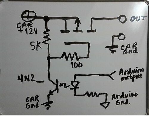
The "opto" could be just about any 4N2_ or 4N3_ device (or whatever with an NPN (photo)transistor output).
The resistor there would be enough to get 10mA or so through the 'LED' (270Ω).

stuart0:
See if these annotations help.

They do! They do! :smiley:

I was thinking in terms of "potentials" (kind of more consequences oriented), rather than biases (I'm being careful to not mis/abuse terminology and am still not 100% clear on "bias"); seeing it from both perspectives is very helpful.

Thank you, Stuart.

I'm still (yeah, I know) wondering how large that 1.5kOhm resistor attached to 12V can be and still have things be reliable? ...and, it gets worse; maybe the resistor attached to the PMOSFET's gate will get moved. See next post.

Cheers!
Dirk

NOSUM:
No you don't want any resistance in the gate leg

This sounds like a generalization - at least for totem poles. I don't have the knowledge or experience to say anything about this, so I'll let you and Stuart hash this one out.

Observation: I've seldom seen the gate/base of a (P)MOSFET/transistor without a resistor before it - totem pole and others. I'm aware though, that this does not say anything about the practice's validity or otherwise.

What if that resistor were moved to occur between 12V and the "upper" NPN's collector? I'm thinking this may upset the "bias balance" (I'm still working on digesting this characterization) so maybe the 1.5kOhm resistor would need to be adjusted to compensate?

NOSUM:
It does not matter that you may not be able to get your head around why it is so, just accept that it does.

Um, if I were to do that, this topic would have been significantly shorter. :wink: Plus, it's not me questioning your assertion; I would be perfectly happy to not have a resistor in line with the PMOSFET's gate. :slight_smile:

PS This difference of approaches between you and Stuart on resistor vs no-resistor on the PMOSFET's gate seems reminiscent of my contention that the "fighting each other" of BJTs in an inverted totem pole occurs in such a small time frame in a circuit with such a low frequency (I can see this would be a larger concern in high frequency scenarios), that it's maybe a worthwhile trade-off in terms of drive capability. I.e. Exactly what percentage of the time are these BJTs "crossing over" (what percentage of time is spent "shooting through")? Now armed with a (little) better understanding of "potentials" or "biases" in such circuits, I'm going to explore this "PNP driving the PMOSFET's gate" possibility some more. (I know, I know; throw the noob a few explain-y tid-bits, and off he goes, getting all promiscuous with the magic smoke... ::slight_smile: )

Cheers!
Dirk

Thank you for joining the party, Runaway!

Started that way, and has progressed to how to best turn a PMOSFET on/off. :slight_smile: ...with a controversy on the niggly-little nuances of whether or not a resistor should be present at its gate whilst executing said "on/off" transitions thrown in for good measure. ;D

I explored using optos early on (I got a bunch of them specifically for this purpose). From what I remember, the transition times for opto are rather long - even for the 500-2500Hz PWM rates I'm after. ...though hopefully it's apparent by now that I have neither the experience or knowledge to back that up. Anyone else think an opto approach may be worth exploring?

Cheers!
Dirk

Do you have the components already?
If so, just build up the circuit.
Start with "low-level" testing and scale upward.

For the most recent circuit suggested in this topic, the only component I'm missing is the 1N4001; I do have some 1N4007s I can sub in for now, though.

Before I set up for another wienie roast, I'd like to have the two remaining concerns sorted out:

  • how large can the 12V-to-upper-NPN resistor be?; and
  • should there be a resistor at the PMOSFET's gate, and if not, where should it occur?
    Cheers!
    Dirk

As mentioned, I'm not sure optocoupling is viable in this part of my project, but I'm also working on power management for it (I'll start a separate topic when I'm ready to explore this further) and have been struggling with how to provide external switching (human-switched) information to the Arduino. Optocoupling is definitely the way to handle this. Thank you for reminding me of them, Runaway. :slight_smile:

Cheers!
Dirk

dephwyggl:
I'm still (yeah, I know) wondering how large that 1.5kOhm resistor attached to 12V can be and still have things be reliable?

Both of the "base" resistors (1k and 1.5k) can be increased to around the 5k to 10k mark without changing the operation too much. Will slow it down just a little.

What do you want to achieve by this? Is it to decrease power consumption? They already only require small 1/4 Watt resistors, and they only draw current (about 13 mA total) when the mosfet is turned on. They draw no power when you're not modulating it.

The problem with that circuit is that the chosen mosfet requires about 50 nC removed from the gate just during the transition (fall time). Your circuit only does this at a rate of about 1 mA and so will take about 50 microseconds. The switching losses start to become the dominate loss at this point, something that the op is trying to avoid.

Dirk: I should point out that at low modulation frequencies like 500 Hz you can still get away with a simple one stage (npn) solution with just a pull up resistor. The resistor needs to be down around say 680 ohms though (might be too much load for the opto though) to keep the fall time under about 5 microseconds and hence keep the switching losses relatively small (compared to the on state loss). A resistor of this value starts to dissipate a bit of power though, so you'd need to go up to around the 1/2 to 1 Watt range.

If you want to give yourself the option to later go with higher modulation frequencies however, then you're better off staying with the "push-pull" (aka current source-sink) driver stage.

Observation: I've seldom seen the gate/base of a (P)MOSFET/transistor without a resistor before it - totem pole and others. I'm aware though, that this does not say anything about the practice's validity or otherwise.

The resistor improves damping but is otherwise often optional. In your case however, once you add the gate zener it is no longer optional as you need to limit the zener current. Otherwise you've got a 1W zener trying to absorb the entire energy of the transient, and there's no guaranty that it can do that and maintain its rated voltage (and not die).

It was mentioned previously (by another member) that you shouldn't use a gate resistor, but instead you should limit the current on the base side of the driver transistors. The problem with this is that it makes the effective gate drive resistance becomes a function of the transistor's large signal current gain Hfe (aka Beta).

Recall that previously you were a little miffed about how we deal with such large variations in this parameter on the transistor data sheet. The truth is that good design always tries to make the overall circuit operation largely independent of hfe, at least over a fairly wide range of this parameter. Making the output resistance highly dependent on hfe is therefore poor design practice.

Below are some references that explain a bit more about the design factors in choosing the gate resistor. Yeah, it's a bit technical I know, but you'll see that the general consensus is that a gate resistor is useful to improve damping in the presence of stray inductance.

Take a look at the formula at the bottom of page 10 of the first reference. Using the parameters of your mosfet you will find that Rg = 13 ohms gives somewhere around optimal damping for a stray source inductance of about 150 nH (this corresponds patch wiring with about 5 to 6 cm loop dimensions). This is the assumption I made in my first circuit (reply #32) where I gave this resistor at 15 ohms. I increased it a little to 22 ohms when you increased the transient supply range and added the zener.

Gate Drive 1

Gate Drive 2

Gate drive 3

Gate Drive 4

stuart0:
Both of the "base" resistors (1k and 1.5k) can be increased to around the 5k to 10k mark without changing the operation too much. Will slow it down just a little.

What do you want to achieve by this? Is it to decrease power consumption? They already only require small 1/4 Watt resistors, and they only draw current (about 13 mA total) when the mosfet is turned on. They draw no power when you're not modulating it.

Got it in one. :smiley: Always conscientious around efficiency - particularly if it doesn't cost too much (in this case, speed). I'm aware they're only of consequence during the on/off transition - though these transitions will be occurring 1960 to 5000 times per second... :slight_smile: I'll cut the difference in half (6.8k for the upper, and 4.7k for the base). Hopefully no cause to haul out the marshmallows...

Again, thank you, Stuart. There is no way I would have made it this far without your - and others' - encouragement, persistence and patience. (Hopefully you'll join in again when I start on the switching and power management bits...)

Cheers!
Dirk

I should have known better than that I'd get only one response from you, Stuart. :smiley:

Thank you very much for all the additional information. I'll review it and try to absorb as much of it as I can. A few comments at the moment:

stuart0:
Recall that previously you were a little miffed about how we deal with such large variations in this parameter on the transistor data sheet.

"Miffed"? Really? "Miffed"?! It was more like why the $%@# can't the laws of physics behave in a way so I don't have to do all this @$#%'n math just get a transistor to turn on the way I want it to?! Then I come around to realizing there are forums out there with contributors who seem to be willing to let me guesstimate and ball-park stuff enough to get it to work. Plus, and certainly not least - participating with y'all in these forums is likely the only reason I'm continuing toward the - essentially - superfluous goal of this project. I am having a blast, and can only hope that everyone else is too. :slight_smile:

stuart0:
Below are some references that explain a bit more about the design factors in choosing the gate resistor. Yeah, it's a bit technical I know, but you'll see that the general consensus is that a gate resistor is useful to improve damping in the presence of stray inductance.

I've seen discussions of this elsewhere (I was rather surprised by NOSUM's insistence that this resistor should not occur at the output of a totem pole arrangement). One of the better rationales I've seen talks about using a pre-gate resistor to prevent ringing when it's driven hard. Again, I don't have enough knowledge or experience with any of this to contribute in a meaningful way. For now, I'll leave in the pre-gate resistor, and if I encounter issues, re-visit how to position it differently. The inductance concerns you mention are far beyond me (sounds - like I've mentioned about other things - a little too analogue-y for me) a the moment.

stuart0:
(reply #32) where I gave this [pre-gate] resistor at 15 ohms. I increased it a little to 22 ohms when you increased the transient supply range and added the zener.

The "transient supply range" is still to be determined (I'm hoping for 10-22V, but it could be closer to 10-30V), and the zener has an added resistor in series with it separate from the pre-gate resistor. ...though I still don't see any issue with having both (provided the zener's operation isn't significantly impacted). Final circuit coming up in a while, and then I'll get started on input (human) switching and power management.

Cheers!
DIrk

dephwyggl:
The "transient supply range" is still to be determined (I'm hoping for 10-22V, but it could be closer to 10-30V), and the zener has an added resistor in series with it separate from the pre-gate resistor.

Yes I noticed that on one of your previous circuits and I meant to comment on it. No you can't do it like that, it increases the zener dynamic resistance too much. Yes, overall you need something in series with the zener to protect it, but it cannot go in series after the gate which it is trying to protect. The resistance (to protect the zener) has to be before the gate.

The whole purpose of a zener is that it has a low dynamic resistance after it breaks down. This is how it holds (clamps) the voltage to a reasonably constant level over a range of reverse current. If you add a series resistance at that point in the circuit then the zener can no longer do its job.

The voltage is no longer clamped correctly and it will increase markedly as the zener current increases. With an 18V zener trying to clamp a gate with an absolute maximum rating of 20V you've got very little overhead to work with. Say you used a 150 ohm resistor as per your previously proposed circuit , if that zener has to divert just 15 mA then your gate voltage exceeds 20 volts.