Background: I’m looking to build a module that acts as a bi-directional switch based on mosfets. Call it solid state relay (SSR) if you like. I will have the module made by a PCB manufactory to then be able to use the module in my other designs by soldering it on top, sandwich style. Very modular. The steering voltage is +3.3-5V and the switched voltage is +/-15V.
To the subject: I’m looking at building it with two N-channel MOSFETS in a back to back configuration, driven by the photovoltaic MOSFET driver technology. The reason I look at this option is that I cannot for my life find a traditional suitable high side mosfet driver that is reasonably priced (sub $2) and in stock. If you know one, please post a link! =)
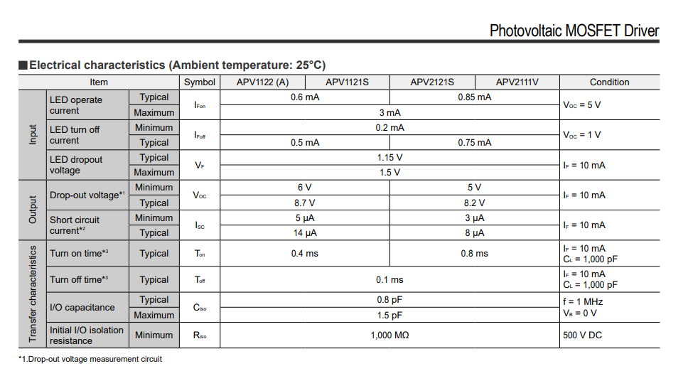
The switch will be turned on 90% of the time, in a battery powered application. This leads me to think about the current consumption of the LED in the driver. The datasheets tend to assume 10mA driving current when they draw up the specs. However I see as low as 0.5 mA mentioned in the specs as well.
How low is it possible to go, and still have the MOSFET guaranteed to be fully on?
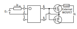
Thank you for reply. Here is a crude schematics. Please ignore that the driver part is illustrated with an inbuilt mosfet, it was the only eagle part I could find. The load will be between PAD1 and PAD2 with a power source in series.
It should work provided that the diodes permanently support the switched current and are cooled sufficiently - see the Diode Forward Voltage in the data sheet. And you provide a voltage source (or Gnd) to the Driver IC.
Draw the driving circuit and you'll see (I did too late) that you build a high side switch and consequently need P channel MOSFETS which can be turned on by a negative voltage (Gnd). Then have a pullup resistor between the gates and drain (to turn off) and insert the optocoupler from gates to Gnd.
Thank you for your suggestion. These IC's has inbuilt MOSFET which means we are constricted to their limits. We need higher currents than what an inbuilt MOSFET can handle.
But it is a N-chan MOSFET based high side switch I'm trying to build. Not a P-chan MOSFET based one. N-chan has lower resistance vs price/footprint/availability. Thats why I need a driver IC, either with a charge pump or by other means rise the voltage, such a photovoltaic IC.
The circuit is drawn up here and can be simulated:
Here is a simulation with the gate voltage taken from 0V to 15V and how the N Mosftes start to conduct and transfer current, in a high side configuration.