So isn't there a solution to get the characteristic I posted earlier of a Vss pin ? I know it's possible since I have this screenshot I posted, but I'm not sure how they did it (I just know the acquisition wasn't with an Arduino, it was with a NI DAQ card but this should change the fact that it's possible with arduino too)
Oh so you mean for future people seeing this subject. Sure I'll make a new diagram as soon as I find the solution for the Vss plot. And then I'll flag it as solution
From that reply, it seems like you're saying you are not sure if your circuit works, or you need to know what will work. Is that the case?
Absolutely not. It is for us, now.
I think my circuit works fine since I get the form of the plots I was expecting. I'm just trying to figure out why the threshold voltage of the diodes inside the SD card are so high, and also if I could get the plot for Vss1 or Vss2, it would be perfect!
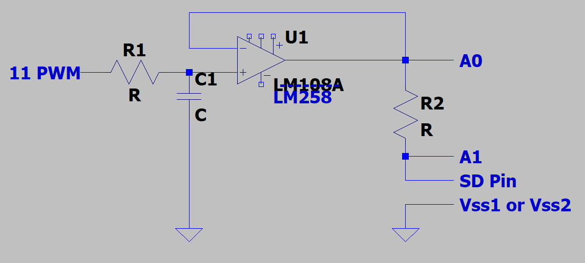
I'm currently making the whole circuit scheme again for you
What was the circuit and equipment used to generate that graph?
How were they connected to the SD card?
There always has to be two connections, where did they make these connections?
1 Like
I cannot reverse engineer the whole tool they used. But I have documentation I can read to try and get that info. I'll keep you posted if I find anything interesting.
The problem would disappear without the resistance but then it would be impossible to know the current in the circuit right? So I don't see any easy solution.
The op amp output may not be capable of reaching 3.3V if powered by 5.0V
" Input common mode headroom (to positive supply) (typ) (V) -1.5
Output swing headroom (to negative supply) (typ) (V) 0.005
Output swing headroom (to positive supply) (typ) (V) -2
1 Like
Also, in best of worlds, I would like to get a voltage going from -3.3V to 3.3V with my PWM so I can plot a whole characteristic with negative values too since there aren't only passive components inside (thus the characteristics isn't always symmetric).
But this seems to be very difficult with Arduino, I didn't do a lot of research yet but it seems even DAC0 and DAC1 outputs support only positive ouputs
I realised that when I tried to read the voltage at the output and it was "only" 2.3V but it should be enough for my use.
Is this test something you only need once, or is it like a test jig that will run 100's of devices all day long?
Or is it something else?
I'm not to sure what that graph is showing.
If the voltage is ZERO how could there be a current?
Your diagrams are fine
You were asked for a complete diagram. You didn't post any, just a re-hash of the first one, complete with cross outs. I'm out. Good luck.
Before I go, I'd like to point out that you should have mentioned this up front.
May I ask what the point of all this is?
The SD card contains complex internal electronics which - as I understand it so far - are not in operation because no supply voltage is applied. Ultimately, only the characteristic curve of the protective diodes is measured. And even that is not really measured, because these diodes are not connected to Gnd, but to the internal electronics (Vdd). In the end, this is phantom powering of the internal electronics via the resistor. I don't see any real sense in this measurement.
1 Like
I wondered about the point of this, as well.
Unless the current flow is limited by some means, one can rather easily destroy unpowered ICs by injecting signals into pins.
I can't say a lot about that but I know that what I'm doing has a meaning. When SD cards are damaged testing electrically each pin can be of huge help before trying to connect it to a computer (a short circuit could damage the card and thus the microcontroller, leaving us with only the possibility of reading the NAND memory directly)
What did you expect when you asked for a "complete diagram" ? I said before that I'm new to this forum and arduino so I genuinely didn't get what you were asking.