I'm trying to plot the current-voltage characteristic of a single pin of a micro-sd card.
I came up with a test circuit with a diode to know where I'm going. I'm generating a voltage between 0 and 3.3V with the PWM mode of my Arduino Due. I also filter the signal with an RC filter (R=15k and C=1uF) and I added a buffer (with an operational amplifier LM258 that I power with the 5V output of the arduino). The output of the amplifier is connected to both the A0 input of the arduino and a resistance (of 270 ohms) so that I have access to the current value in my circuit. I then connected a diode and another pin A1. Doing A0-A1 thus gives me the voltage Ur of the resistance and I retrieve the current with I=Ur/R. A1 gives me the voltage of the diode so that I have all the information I need for the characteristic.
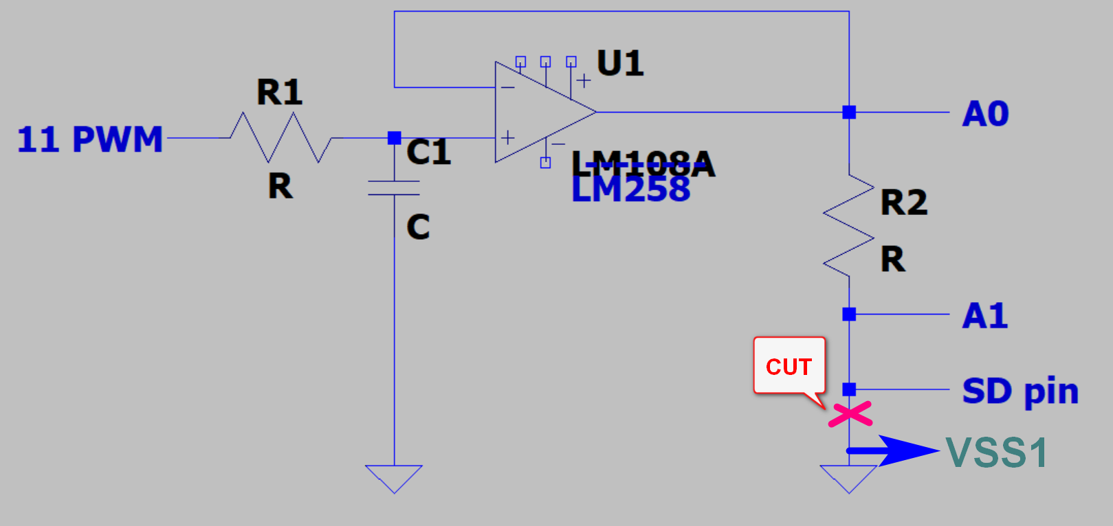
To make everything clear, here is the imaged version of the circuit I made on my breadboard :
All the raw digital values are sent to the serial port. Then with pyserial library in Python, I read them and I plot them with matplotlib.pyplot library.
Everything seems to work with the diode as you can see with this plot :
The thing is, an SD pin isn't a dipole, so I just can't wrap my head around finding a solution on how to adapt this circuit to receive this pin. The answer seems obvious and easy but I just don't get it. Here is the only test I did by just connecting the pin to get the potential with A1 :
And it gives me this characteristic which just seems to be the characteristic of the resistance.. and that's quite logical : [I'm a new user on the forum so I can't upload more than 3 images, I'm gonna try putting it in the comments but it's basically a line, looks like the characteristic of a resistance with a 1/R coefficient]
If anyone has an idea I'd be happy to hear it!
Thanks,
I was expecting to see something like this :
since Vss1 is the GND
I just feel like I'm missing the whole point here but can't figure out what it is
Of course, a potential needs a reference and here I'm assuming that's where the problem is, the reference is my GND on the arduino board but my SD card isn't connected to this GND or any reference.
What I'm trying to say is that the 3rd pin of an SD card is Vss1, so in the normal utilization of an SD card, it would be connected to the GND. But here I'm just connecting it as shown so of course it makes a short circuit to the ground, meaning I'm just plotting R2.
That's where my question is, how can I get the plot I uploaded ? So I can get the characteristic of this pin and the others too ?
Exactly, I'm trying to get the characteristic of ONE pin. And repeat the process for every pin. I am not making the characteristic of one pin regarding another.
But of course, I need a voltage to make a characteristic meaning I need two potentials, so I just went ahead and referenced everything with the GND of my board, but maybe that's not how that works and there's the point I couldn't be able to understand alone. What are you suggesting?
EDIT : I'm quite new with arduino boards (been using them for a month now) I'm a lot more familiar with the NI environment with their cards and softwares (LabVIEW, CVI etc...) so I could also be totally wrong about how I'm using the arduino too
Thank you so much for your answer now I see where you're going. Of course I wasn't connecting my SD card to the ground... Now I get the kind of plots I was expecting to see, for example for the DAT0 pin:
It's basically the characteristic of a diode but that's because as often in electronics, these pins have a protection for high voltage inputs and these things are made with a diode.. It's just the threshold voltage of the diode that seems a bit high to me, I was expecting to see like less than 1V.
Problem is, there is a second "Vss2" pin connected to the ground, and so it's also connected to Vss1... Thus when I'm trying to plot the pin Vss2 I get the characteristic of the resistance... :
What do you mean ? Like when I posted the corrected circuit by jim, I should've posted the whole circuit ? Nothing changes before the op amp since everything regarding the signal conditionning seems to work fine. Sorry I was lazy and didn't want to draw a scheme of the whole circuit all over again (I didn't save the first one).
The pin characteristics need to be measured relative to some common point, in this case Vss.
Since Vss1 and Vss2 are the same you just get the resistance
It's not important what happened before. It is important to get everything in one place now. There is too much guesswork in putting all the separate diagrams and statements together. Please make a new diagram.