I made a testbed for this ESP32. Everything is fine until it comes to connectivity. WiFi scan example throws burnout. So it is the power issue.
According to this schematic, I used the right capacitors on the power rail. That means 100nF and 10uF.
As it works stable at blinking LED, etc, it obviously doesn't work as it should when there is some bigger current draw. I used 0603 caps, not sure of tolerance. It might be a problem with their position. 10uF cap is close to pin 46 (VDDA) and 100nF is close to pin 19 (VDD3P3_RTC). Yeah, I know, this last I did by mistake. Maybe I should take this one and put it on top of the 10uF. But is it the right place at all?
What should be the best solution for power rails, caps, etc, to avoid these current issues?
Edit:
I put this 100nF on top of the 10uF on pin 46. Still have power issues.
Edit 2:
I noticed that when it blinks, it has a normal temperature. When it tries to scan WiFi networks and get those resets, it gets a little warmer.
It is a custom board, the schematic will follow later. I am not at my pc right now.
I power it over a USB from a PC. Onboard, there is a CP2102. What is weird is when I upload a WiFi scan example and it goes to these resets, I lost it on my COM port. I have to press the reset button, in time to upload any other sketch.
Another thing, there are some additional sensors onboard, HDC1080, etc and they work just fine. This is my first design with this chip. I might miss something.
Just to mention, no matter the other components, in my initial tests with WiFi, there were only ESP32 and CP2102 with what is necessary to work with.
If we knew what that was, we might be able to assist.
Most important is that the antenna section of the ESP has absolutely no materials, particularly copper traces but even PCB laminate, anywhere near it, underneath, above, beyond or to either side.
"Near" means several centimetres. So the antenna section must overhang all other parts of the arrangement.
Sounds like a power problem.
An ESP32 draws a lot of current when the radio is used. The problems you're describing also happen when a long/thin USB cable is used with a factory-made board.
For a custom board I would at least use 470uF tantalum on the output of the 1117, and an additional 100n near the ESP module.
Post a picture of the board.
Leo..
Something that I don't understand is no matter if the antenna design is poor, how will it affect power issues? I don't say it doesn't, just I don't understand why. My guess is if the design is poor, it will affect RF functions. But the fact is, when I use the radio, it gets warmer and stops working. So it is related for sure.
When using this kind of antenna, it says PCB must be 0.6mm thick. According to what I can see, PCB must be 0.6, and the antenna must be placed 1cm far away from everything, at the edge of the PCB.
What trace width should I use? I use 0.254mm
Everything else I try with the board works like a charm. As I said, this is just for testing. To see how it works. Maybe eventually to design something useful in the future.
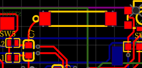
Sorry, but everything I see there is a total RF design disaster!
There are tracks running under C7, the end of the antenna is next to SW3, there is a long track running from I.1 and I.2 - whatever they are - to somewhere else, a blue track parallel to the antenna and the antenna is located within the PCB outline.
None of these components must be anywhere near C7 and the antenna, and the track between the ESP and the antenna must be correctly designed with the correct PCB material and rear groundplane with correct ground "thrus".
Let's say the ESP32 with a network connection is programmed to transmit. The radio is in lower power state to receive data but when the radio is ramped up to transmit there is a sudden current draw. Depending upon the load being placed upon the ESP32's regulator, the sudden current draw may cause brownout issues in other components attached sourcing power from the ESP32.
If the radio starts off good and gets hot as its used, the ESP32 and in this case the board could be defective.
An antenna for an ESP32 can be a 4 inch length of 30AWG wire soldered to the center pin of the connector. Trim the wire in 1/32 increments for tunning. It's not the best but it does work.
Are L1/L2 directly connected to a ground plane. If not, then the Pi filter won't work as intended.
Why didn't you use an ESP32 module, where the tricky (black art) parts are already solved for you.
Leo..
It doesn't help the OP but I am also curious about the design decision to use a raw esp32 chip instead one of the tiny modules which incorporate the chip plus ancillary components plus antenna. This, for example, is available say from Mouser for a couple of $ and is about 20mm by 15mm : https://www.mouser.ch/datasheet/2/891/esp32_s2_mini_1_esp32_s2_mini_1u_datasheet_en-1928084.pdf
It works great if there is no RF. It gets hot with a simple wifi scan example. Which resets the board. I will take a look at the link you provide.
There is no ground plane. I can make a revision or shorten the GND path with a wire if that will do any good.
I used this one because I want to learn. There are many designs with this chip, and they work. I just want to make my own design that will work. And maybe in the future, it could be used in something useful.
ESP32 modules are ok to me. I used them in all my projects. But as I said, I made a successful design with a barebone ESP8266EX, why shouldn't do the same with this D4?
"anywhere near" meaning within about 1 wavelength which is 12.5 cm.
In other words, there must be a plane - an effective flat surface - from which the antenna projects, which is clear of all obstructions. Any encroachment will degrade the performance and if sufficiently degraded, will reflect most or all of the power back into the transmitter as you have experienced.
A good example of an antenna design is the little whip projecting up from the roof of a car.
According to Paul_B suggestion, there must be some redesign. I will try it and before ordering it, I will post it here. Just to make sure if I did it right.