ESP8266/ESP-12F EXPERT NEEDED: Having issues replicating the Wemos D1 Mini V2's use of the ESP-12F, difficulties flashing firmware

I'm currently working on a custom PCB design that uses a portion of the WeMos D1 Mini V2's schematic for the microcontroller aspects of it. I chose this specific design for the removal of a need for a dedicated FLASH button. From the two test PCBs I ordered from JLCPCB however, both connect via USB and are recognized by serial monitoring, but one PCB only flashes when the RESET button is pressed exactly at the start of the flashing process, and the other refuses to flash entirely.

Shown here is my implementation of the ESP-12F:

This is the tool I'm using to flash these PCBs: https://slimevr-firmware-tool.futurabeast.com/

I've asked around in several other places already but I'm having trouble finding someone who knows the ins and outs of this stuff well enough. I reply more quickly on my discord, Radiant#3831, but any help either here or there would help tremendously.

Shown here is the schematic I'm trying to recreate, minus the stuff I believe I don't need.

bumping since I still haven't figured this out

I've been busy. And a bump after a day is fine I hate schematics like this, connect the wires properly for me and focus on the connection to of GPIO0 i would like to say. I would not try to copy someone else's board, I mean, do you actually need the whole USB thing ? Just wasted space and components.
I just have a 5 pins for the upload VCC TX RX GND GPIO0 and only have the voltage divider on the rx-line on-board.

Anyway, the original schematic lacks resolution. (and as said i hate those schematic with all those tabs, you can't see where anything really goes but have to look for the corresponding tab.)

The issue must be related to GPIO0 and the DTR system so let's focus there.
Your comment below the DTR system is an indicator that you have found a solution for an issue, While really i guess you should create the Symbol and the corresponding footprint if it doesn't exist in the library you have, and then create PCB.

Can you check in the gerber that the correct pins are connected to the proper tabs ? If you have it in the schematic as 2 individual transistors how does that translate into a dual-package footprint ?

I'm not sure what you mean by "do you actually need the whole USB thing". Considering that this is how you install/update firmware, as well as being able to change the wifi settings on the board, I would assume that this is a vital feature of my device. Especially considering that this not just for me to be able to do this, this is a product I will be making several of.

As for the footprint, EasyEDA screams at you whenever you're not using the name/footprint provided by their system for a specific part, so it's much easier to specify what's wrong with the footprint provided instead of trying to modify it yourself.

The pins are connected properly, EasyEDA also screams at you when that's not the case. I'm not sure what you mean by "dual-package footprint".

Hopefully this image shows more clearly what the circuit I'm referencing uses.
Imgur

To clarify on why I need this schematic, the product I am creating is a variant of SlimeVR, an open source solution for affordable full-body tracking for VR. These can easily be built using schematics provided by the SlimeVR docs. My specific design references the variation of this schematic which uses the BMI160 and Wemos D1 Mini. Thus, I need to reference it to maintain consistency in terms of the hardware/firmware used by 99% of the SlimeVR community.

As for why everything isn't directly wired together on the board this is mainly to give each trace of the PCB a name that isn't generated by the software, making routing those traces much less confusing.

Yes but in your schematic Q1 & Q2 are separate symbols, rather than parts of the same symbol. How can 2 symbols share 1 footprint ?

That is an EasyEDA quirk then, i use Kicad with different quirks.

one could use a programmer, but you choose to have the programmer 'onboard'

can you show me the gerbers ? clearly something is not going right with the DTR, at least when you are attempting to use exactly the same process on your PCB as with an 'genuine' Wemos.

In the original schematic they use a UHN3N
You use 2x LMUN2233.

Yes but verification of the schematic becomes harder since 1 tab may be connected to several other tabs. I don't have the software, where selecting 1 tab lights up all other tabs with that same name.

So what firmware do you actually load onto the Wemos ?

Does it work if you manually ground GPIO0 and press the reset button ?

That would also require DTR not to trigger RST unless you keep GPIO 0 Grounded.

They don't, Q1 and Q2 are separate parts. The thing that's wrong with their footprint is that each one has a built-in resistor that isn't shown.

Right, because I want consumers to be able to mess with the firmware without the need for a separate programmer accessory. USB-C on the outer case shell makes way, way more sense to have than a JST connector or something, especially considering this device also needs a way to charge.

It seems like I'm too new of a user to be able to upload attachments other than photos.

I mentioned this in the first message.

That is the flash tool, you can upload any binary with that.

Now i have not a clue anymore why you want to create your own Wemos ? What you want exists, and to create it yourself is rarely going to be cheaper.

So anyway, that's where the modification on the original is. The original also has a device with the internal resistor, that is the same, you use 2 parts, the original uses one. I guess you picked the right part.

And a gerber file can be converted to a PNG ? (i use my screenshot as a converter) But yes, that is an annoying limitation to discourage Spam.
I will just keep replying that should remove the limit as soon as possible.

Now i suspect that you intend to use LiPo's for that, well that is a completely different matter i guess.

This flash tool only lets you use SlimeVR firmware. I'm using the firmware included with this tool.

To reduce product size. It's much easier to integrate an ESP-12F and TP4056 into a PCB that fits around a 1/4-20 threaded insert in a case no taller than 16mm or wider than 60mm than it is to fit the pre-existing boards for each. The BMI160 board I'm using is an exception, since it's just barely small enough to fit inside and having JLCPCB install the BMI160 chip for me would make each device cost twice as much, for whatever reason.

Worth mentioning as well, so long as I buy these pre-assembled PCBs in bulk, this is MUCH cheaper in material alone, not to mention the time I would be saving not having to attach a D1 Mini to my board myself. I know this because I already tried it, this version of my device is the 4th iteration.

Here, lets see if this works. https://drive.google.com/file/d/11ab9glyE5Fjp1of9zgxNEZeQz3eSvkvP/view?usp=sharing

Yes. These are wireless full-body trackers for use in virtual reality, so the ability to be wireless is very important.

Now that makes sense.

Well i figured that much, but the 'different matter' comes to light now. Using a TP4056 for charging, how do you prevent 'load-sharing' ? in other words, how do you prevent the board from draining current while the battery is being charged ? It is something to consider for safety. You have been creating a board, so i guess you thought about it, but given this kind of info, i just have to ask (check).

No, i don't use google-drive, but i would need to sing into something.

That happens. I make boards that use mosfets, If i want JLCPCB to add them to my board, i need to buy 2500 of them first up. My boards are not that successful yet.

But this is the first time you are using an ESP12-f rather than a Wemos ?

Anyway we are drifting off. (my fault) The issue must be somewhere in the automated Reset system, either in the 2 transistors responding to DTR and pulling GPIO 0 LOW while pulling RST LOW, and otherwise further upstream (so to say) in the CH340. As said, i don't use the automated reset system on my boards, but rather do the initial upload and use OTA from then on.

Ah well that is a limitation that wasn't clear to me. I guess it works with original Wemos, so it should work with your board.

Hmmm how to figure out what is going on, even with an oscilloscope, i guess you would need to monitor several pins to see if what is supposed to happen actually does.

Maybe the easiest is the sacrifice a PCB, remove the transistors, and create 2 push-buttons (or just one, i see you actually have a RST button already) to set the board into 'flash-boot-mode' manually, so at least you can confirm that the whole rest of the board works as it is supposed to.

There is also the possibility that JLCPCB or you have made a mistake with the BOM of course, The Capacitor on the RST pin might not be the correct value. If that is to big, you would have to manually reset the board every time because the DTR signal won't manage to pull the Pin LOW. For a manual reset system, it doesn't need to be there, and even for an automatic one, i think it should work without (or it is in the wrong place in the schematic and belongs to the DTR system) , so it's worth a go to remove it and / or replace it with a cap if which you know the size.

I am just throwing Ideas in there, if you can open your gerber viewer and make a screen-shot for each layer, then crop them, you can post the gerbers as pictures.

I have already done a bit of probing. At at least in the case of the PCB that entirely refuses to flash, DTR does manage to pull low consistently, but RST never automatically changes, and RTS seems to go between 0.8V and 2.8V, instead of what I would assume to be the expected 0V and 3.3V.

I'm hesitant to any disassembly of these assembled PCBs, mainly because I don't have the proper equipment to work with SMD components this tiny.

a 10x magnifying glass, tweezers and a small blower soldering blower.

I want to encourage you to remove what is C3 on your board, you should be able to heat both sides with just a single soldering iron that has some fresh solder with flux on there, no blower required. I actually find SMT parts easier to replace than THT, but for parts with more than 2 pins a blower is a lot easier. Depending a bit on the quality of your eyesight, you may get away with the 3x magnifier that comes with the standard 3rd hand.

The capacitor may be holding it HIGH.

If you want to put it back on the board, you will not find that very hard to do.

The transistors do have some voltage drop. It should be easily enough for the logic level required.

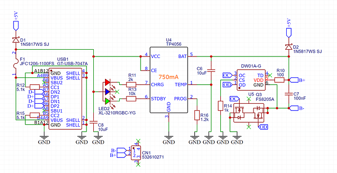
About the Gerber. Yes i can see them now, but stuck with some questions. What is Q3 ? i can not find it anywhere in the schematic and i suspect it's the soic-8 package in which Q1 & Q2 are printed on the silk layer and Q1 & Q2 are actually right next to it ? It has gotten a bit messy, but if you get it manufactured, that isn't all that important i guess. The mixture of different packages for the resistors, and the shape not inviting to group them. Anyway let's focus on Q1 & Q2, are you sure they are rotated correctly and are the correct part ? Manufacturing can be extra tricky that is why i tend to do just a PCB batch without the parts, but with parts i have, like that i can confirm that the schematic actually works. How many did you make ? About the size of the PCB, you didn't you the back of it for parts placement, that is where you can save a huge amount of space ! At JLCPCB they don't care which side you put the parts, anyway maybe next time.

Q3 is part of the second schematic for this PCB that shows the implementation of the TP4056.

The traces match up in EasyEDA, so I'm assuming yes.

Two, and both show different behavior. One only flashes with correct timing of the press and release of RST, and the other refuses to flash.

The flat side is to make it easier to place inside it's case, but I was also under the impression that there was a cost increase for double-sided assembly.

I suspected as much. Other than that you did not provide complete information from the very get go, how are you drawing 5v from a LiPo, i mean there must be a buck converter somewhere ? a Lineair regulator is just not going to work ah i see the 6211, well that states in the datasheet Vin = Vout + 1V, so if you want 3.3v for the ESP, you will need 4.3v minimum, and the LiPo will not provide that.

btw, if you have prog at 1.2K that means that you will be charging at the 1A (not at 750mA as stated) and now i see why USB C is required. Are the 1N5817 diode talking care of the load sharing issue ?

We need to know for sure. Check the connections with the multimeter.

And no prototype at all i guess. Hmm disappointing. I would start with the one that isn't working at all and pull those transistors off. It is useless as it is and it should work. Best to try and set it to flash mode manually. They are close enough to the edge off the board that you can get to them. It is likely that the transistors are just not working the way they are supposed to, they may not fully saturate or they may already be faulty, can you post the link to the part in the JLCPCB part library ?

Some yes, they need to make a second stencil for the paste, but the amount is not major. It's a design choice, there is so much space on the back underneath the bigger components, that i usually find it worth it, but then again, i start out manufacturing myself.

Anyway i guess you understand that i have a different process of getting to an end-product than the process you chose. Obviously to prevent these kind of mishaps.

Anyway, power wise, a MT3608 is a much better choice to achieve 3.3v from the range input voltage that you have. Admitted that it is more expensive (it's more parts), but even 3v input will result in 3.3v output if you use the proper resistor values.