Hi, i have this circuit that i made, that is a 433mhz radiocontroller, with 3 buttons. It is powered by a battery, so i made the circuit that only when a button is pressed, the battery is connected. I printed this. The problem is that it is not working (let me explain after images).
This is the circuit:
(the pin 3 of the crystall is attached to GND, i forgot about it, but i soldered a wire and now it is attached to GND).
This is the front of the PCB i printed:
This is the back of the PCB:
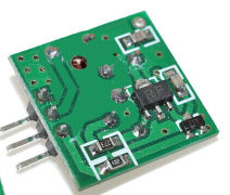
this is the Transmitter module that I disasembled to place in my PCB:

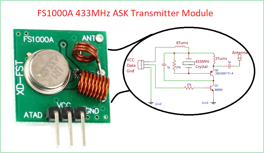
Schematic taken from: this image
The problem is that the receiver (the module100% works) is not receiving any signal. For the project i used a custom RadioHead library, that can be found on this github: GitHub - vlastahajek/RH_ASKTiny: RH_ASK from RadioHead optimized for ATtiny
i don't really get where i'm wrong.
Please explain the purpose of D1 and D2, which (approximately) short circuit the battery to ground.
What is "Vcc" on the schematic?
As presented, the schematic does not represent a workable design.
They are not shorting. Since i want that if Button 1 (SW1) is pressed, the attiny85 will know that Button 1 (SW1) is pressed, and not Button 2 (SW2). In this way if I press the first button, the HIGH signal voltage will only go in in PB3 and not in PB4.
I have to do this since 3v3 is connected in both buttons, and attiny85 will detect PB3 and PB4 HIGH.
Sorry, I incorrectly interpreted the schematic.
The diode connection to Vcc is problematic, as the forward diode drop of about 0.7V wastes a considerable fraction of the battery power.
strange because if i attach an external 433mhz module to the pin PB1 and VCC and GND, it works, it transmitt data without problems.
The design of very high frequency RF circuits is not at all trivial. Just changing the board layout changes stray capacitance values, which can easily prevent the circuit from oscillating.
Also, the specified ME2108A33PG step up converter produces 3.3V, not 5V.
The output of the step up, is actually 5.5V (measured with my multimeter)
Sounds like there are several different problems.
Could you help me find out?
If the 433 MHz circuit is not oscillating then the PCB design itself is likely the problem, and calls for rearrangement of the parts. Get that part working on smaller test PCBs that will then fit into the larger plan without significant changes in the copper layout.
RF circuit design is normally done by trained engineers with many years of experience and a full complement of RF test equipment. They may have to make several boards to get the device working according to specifications.
Ok so i will try to do this schematics without the pcb, if it still doesn' work, i will just put 3 holes up the pcb, where i will be able to attach a 433mhz module.
Otherwise another idea i got is that I could use this module that is significally smaller then the normal green. The normal green square is 2cm x 2cm large, meanwhile this blu smaller one is 12mm x 15mm. I could make the pcb in that way that i can attach this smaller module.
Doing in that way, so noo more problem of transmitter module. Would you suggest any other changes to make to the PCB? for example, can the step up be okay? Is my diode system suitable for understanding which of the two buttons is pressed?
Likely the problem is that the original is using the capacitance of the copper on both sides of the board to tune the circuits. Your design did not include that capacitance because it is NOT part of the schematic, but is part of the design.
Hi,
The two inductors should be as close as possible to each other and where they join should be as close as possible to the crystal.
You have the transmitter circuit spread all over the PCB, look very closely at the component layout on the original transmitter.
Tom.. 


 strong text****strong text
I already mentioned problems with both subcircuits.
Ok i understand. Sorry for taking your time. I will use an external module. By the way, there is not any short in my circuit, it works fine. And VCC is the "output from the button", because i jsut wanted to separete the 3v3 from the battery with what is after the button.
The "Battery & switch" and "Boost converter" subcircuits below are examples of how professionals do a coin cell push button remote. Plenty of decoupling capacitors, and Q1 is essential for getting the most out of the battery.
I don't know if it is important, but that type of battery only delivers 3V. And if you use a Schotty diode you will have less voltage drop.


