How to read more than 8 cascaded shift registers with SPI?

Dear Community,

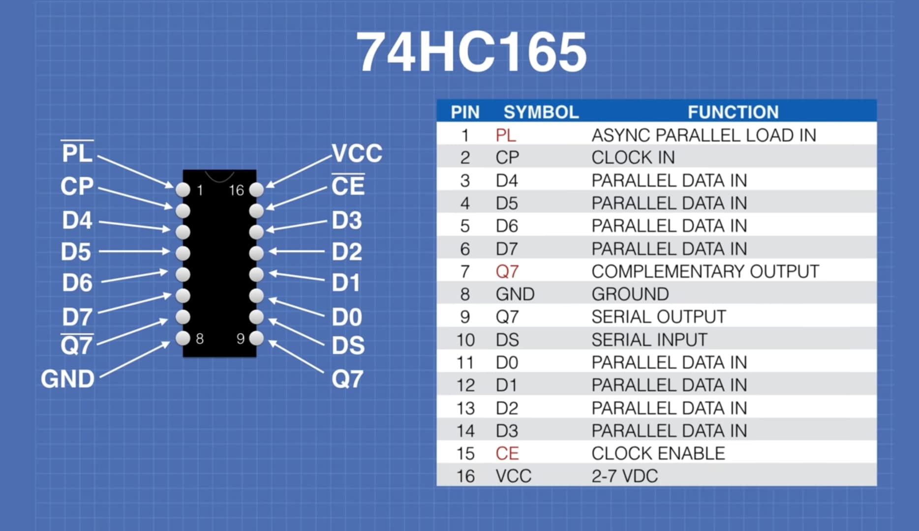
I have a cascade of 9 PISO (74HC165) shift registers connected to an Arduino Micro.
I would like to read 9 bytes of inputs.

Using the shiftIn() function, I was only able to read the data of the first 4.
Using SPI, I can reliably read the first 8. Unfortunately, the data of the 9th shift register only appears 8 times at the beginning, than it shows "0" for the rest of the time.
If I reupload the code, it shows "0"-s right from the beginning (for the 9th one only, while displaying valid data from the first 8).

Here is my code:

#include <SPI.h>

// Define Connections to 74HC165 -- Switch INPUTS shift register cascade
byte ssPinButtons = 10;  //Load for 74HC165 shift regs.

// Define other variables of the code
byte switchStates[9];


void setup() {
  // Setup Serial Monitor
  Serial.begin(9600);
  
  // Setup 74HC165 slave select
  pinMode(ssPinButtons, OUTPUT);
    
  SPI.begin(); // default settings: 4 MHz clock, MSBFirst
}

void loop() {  
  // Get data from 74HC165
  digitalWrite (ssPinButtons, LOW);
  digitalWrite (ssPinButtons, HIGH); // capture data
  SPI.transfer(&switchStates,9); // read in 9 bytes
  
  // Print to serial monitor
  Serial.print("Pin States -- 1 -- 1-8:\r\n");
  Serial.println(switchStates[0], BIN);
  Serial.print("Pin States -- 2 -- 9-16:\r\n");
  Serial.println(switchStates[1], BIN);
  Serial.print("Pin States -- 3 -- 17-24:\r\n");
  Serial.println(switchStates[2], BIN);
  Serial.print("Pin States -- 4 -- 25-32:\r\n");
  Serial.println(switchStates[3], BIN);
  Serial.print("Pin States -- 5 -- 33-40:\r\n");
  Serial.println(switchStates[4], BIN);
  Serial.print("Pin States -- 6 -- 41-48:\r\n");
  Serial.println(switchStates[5], BIN);
  Serial.print("Pin States -- 7 -- 49-56:\r\n");
  Serial.println(switchStates[6], BIN);
  Serial.print("Pin States -- 8 -- 57-64:\r\n");
  Serial.println(switchStates[7], BIN);
  Serial.print("Pin States -- 9 -- 65-72:\r\n");
  Serial.println(switchStates[8], BIN);
  
  Serial.print("\r\n\r\n");
  
  delay(500);
}

If I unplug and replug my Arduino to the PC, I get the following output on the serial monitor:

  1. Zeros
  2. Mostly "1"-s, but not everywhere - this part is also a bit different (seems random) for every try
  3. Two times of semi-valid data (shift registers 6-9 give "0"-s only)
  4. Perfectly valid data for 8 times!
  5. Valid data for the first 8 shift registers only; "0"-s for the 9th one, from here on...

...
Pin States -- 1 -- 1-8:
0
Pin States -- 2 -- 9-16:
0
Pin States -- 3 -- 17-24:
0
Pin States -- 4 -- 25-32:
0
Pin States -- 5 -- 33-40:
0
Pin States -- 6 -- 41-48:
0
Pin States -- 7 -- 49-56:
0
Pin States -- 8 -- 57-64:
0
Pin States -- 9 -- 65-72:
0

Pin States -- 1 -- 1-8:
101000
Pin States -- 2 -- 9-16:
11111111
Pin States -- 3 -- 17-24:
11111111
Pin States -- 4 -- 25-32:
11111111
Pin States -- 5 -- 33-40:
11111111
Pin States -- 6 -- 41-48:
11111111
Pin States -- 7 -- 49-56:
11111111
Pin States -- 8 -- 57-64:
11111111
Pin States -- 9 -- 65-72:
11111111

Pin States -- 1 -- 1-8:
101000
Pin States -- 2 -- 9-16:
10111110
Pin States -- 3 -- 17-24:
11111110
Pin States -- 4 -- 25-32:
0
Pin States -- 5 -- 33-40:
10000000
Pin States -- 6 -- 41-48:
0
Pin States -- 7 -- 49-56:
0
Pin States -- 8 -- 57-64:
0
Pin States -- 9 -- 65-72:
0

Pin States -- 1 -- 1-8:
101000
Pin States -- 2 -- 9-16:
10111110
Pin States -- 3 -- 17-24:
11111110
Pin States -- 4 -- 25-32:
0
Pin States -- 5 -- 33-40:
10100000
Pin States -- 6 -- 41-48:
0
Pin States -- 7 -- 49-56:
0
Pin States -- 8 -- 57-64:
0
Pin States -- 9 -- 65-72:
0

Pin States -- 1 -- 1-8:
101000
Pin States -- 2 -- 9-16:
10111110
Pin States -- 3 -- 17-24:
11111110
Pin States -- 4 -- 25-32:
0
Pin States -- 5 -- 33-40:
10100000
Pin States -- 6 -- 41-48:
11110
Pin States -- 7 -- 49-56:
1
Pin States -- 8 -- 57-64:
10111111
Pin States -- 9 -- 65-72:
11111

Pin States -- 1 -- 1-8:
101000
Pin States -- 2 -- 9-16:
10111110
Pin States -- 3 -- 17-24:
11111110
Pin States -- 4 -- 25-32:
0
Pin States -- 5 -- 33-40:
10100000
Pin States -- 6 -- 41-48:
11110
Pin States -- 7 -- 49-56:
1
Pin States -- 8 -- 57-64:
10111111
Pin States -- 9 -- 65-72:
11111

Pin States -- 1 -- 1-8:
101000
Pin States -- 2 -- 9-16:
10111110
Pin States -- 3 -- 17-24:
11111110
Pin States -- 4 -- 25-32:
0
Pin States -- 5 -- 33-40:
10100000
Pin States -- 6 -- 41-48:
11110
Pin States -- 7 -- 49-56:
1
Pin States -- 8 -- 57-64:
10111111
Pin States -- 9 -- 65-72:
11111

Pin States -- 1 -- 1-8:
101000
Pin States -- 2 -- 9-16:
10111110
Pin States -- 3 -- 17-24:
11111110
Pin States -- 4 -- 25-32:
0
Pin States -- 5 -- 33-40:
10100000
Pin States -- 6 -- 41-48:
11110
Pin States -- 7 -- 49-56:
1
Pin States -- 8 -- 57-64:
10111111
Pin States -- 9 -- 65-72:
11111

Pin States -- 1 -- 1-8:
101000
Pin States -- 2 -- 9-16:
10111110
Pin States -- 3 -- 17-24:
11111110
Pin States -- 4 -- 25-32:
0
Pin States -- 5 -- 33-40:
10100000
Pin States -- 6 -- 41-48:
11110
Pin States -- 7 -- 49-56:
1
Pin States -- 8 -- 57-64:
10111111
Pin States -- 9 -- 65-72:
11111

Pin States -- 1 -- 1-8:
101000
Pin States -- 2 -- 9-16:
10111110
Pin States -- 3 -- 17-24:
11111110
Pin States -- 4 -- 25-32:
0
Pin States -- 5 -- 33-40:
10100000
Pin States -- 6 -- 41-48:
11110
Pin States -- 7 -- 49-56:
1
Pin States -- 8 -- 57-64:
10111111
Pin States -- 9 -- 65-72:
11111

Pin States -- 1 -- 1-8:
101000
Pin States -- 2 -- 9-16:
10111110
Pin States -- 3 -- 17-24:
11111110
Pin States -- 4 -- 25-32:
0
Pin States -- 5 -- 33-40:
10100000
Pin States -- 6 -- 41-48:
11110
Pin States -- 7 -- 49-56:
1
Pin States -- 8 -- 57-64:
10111111
Pin States -- 9 -- 65-72:
11111

Pin States -- 1 -- 1-8:
101000
Pin States -- 2 -- 9-16:
10111110
Pin States -- 3 -- 17-24:
11111110
Pin States -- 4 -- 25-32:
0
Pin States -- 5 -- 33-40:
10100000
Pin States -- 6 -- 41-48:
11110
Pin States -- 7 -- 49-56:
1
Pin States -- 8 -- 57-64:
10111111
Pin States -- 9 -- 65-72:
11111

Pin States -- 1 -- 1-8:
101000
Pin States -- 2 -- 9-16:
10111110
Pin States -- 3 -- 17-24:
11111110
Pin States -- 4 -- 25-32:
0
Pin States -- 5 -- 33-40:
10100000
Pin States -- 6 -- 41-48:
11110
Pin States -- 7 -- 49-56:
1
Pin States -- 8 -- 57-64:
10111111
Pin States -- 9 -- 65-72:
0

Pin States -- 1 -- 1-8:
101000
Pin States -- 2 -- 9-16:
10111110
Pin States -- 3 -- 17-24:
11111110
Pin States -- 4 -- 25-32:
0
Pin States -- 5 -- 33-40:
10100000
Pin States -- 6 -- 41-48:
11110
Pin States -- 7 -- 49-56:
1
Pin States -- 8 -- 57-64:
10111111
Pin States -- 9 -- 65-72:
0

Pin States -- 1 -- 1-8:
101000
Pin States -- 2 -- 9-16:
10111110
Pin States -- 3 -- 17-24:
11111110
Pin States -- 4 -- 25-32:
0
Pin States -- 5 -- 33-40:
10100000
Pin States -- 6 -- 41-48:
11110
Pin States -- 7 -- 49-56:
1
Pin States -- 8 -- 57-64:
10111111
Pin States -- 9 -- 65-72:
0

Pin States -- 1 -- 1-8:
101000
Pin States -- 2 -- 9-16:
10111110
Pin States -- 3 -- 17-24:
11111110
Pin States -- 4 -- 25-32:
0
Pin States -- 5 -- 33-40:
10100000
Pin States -- 6 -- 41-48:
11110
Pin States -- 7 -- 49-56:
1
Pin States -- 8 -- 57-64:
10111111
Pin States -- 9 -- 65-72:
0

Pin States -- 1 -- 1-8:
101000
Pin States -- 2 -- 9-16:
10111110
Pin States -- 3 -- 17-24:
11111110
Pin States -- 4 -- 25-32:
0
Pin States -- 5 -- 33-40:
10100000
Pin States -- 6 -- 41-48:
11110
Pin States -- 7 -- 49-56:
1
Pin States -- 8 -- 57-64:
10111111
Pin States -- 9 -- 65-72:
0
...

This is what I'm expecting to see continuously (without modifying my buttons' states):
...
Pin States -- 1 -- 1-8:
101000
Pin States -- 2 -- 9-16:
10111110
Pin States -- 3 -- 17-24:
11111110
Pin States -- 4 -- 25-32:
0
Pin States -- 5 -- 33-40:
10100000
Pin States -- 6 -- 41-48:
11110
Pin States -- 7 -- 49-56:
1
Pin States -- 8 -- 57-64:
10111111
Pin States -- 9 -- 65-72:
11111
...

Please can anyone help me? I've been looking for solutions in several forums but could not find anything helpful yet.

Perhaps you didn't post any hardware information like a schematic, in those several forums. You seem to have supreme confidence in your hardware, since you are focusing on the sketch. Why?

1 Like

Get the bytes with something like this:

  digitalWrite (LATCH, LOW);    // pulse the parallel load latch
  digitalWrite (LATCH, HIGH);
  switchBank1 = SPI.transfer (0);
  switchBank2 = SPI.transfer (0);
  switchBank3 = SPI.transfer (0);
  switchBank4 = SPI.transfer (0);
etc.

I mean I was just looking for SPI-related issues on this and other forums. This is the first time that I publish my problem and question.

This is my schematic for the connections. I know it's not a standard schematic, I just created this for myself before, but this is what I can quickly share now.

I'm currently not using the 74HC595 shift regs. (but when I use them too, there is no difference).

Connections to Arduino:

  • Green line -- connected to SPI SCLK pin of Arduino
  • Blue line -- MISO
  • Yellow line -- slave select (I chose pin 10 of my Arduino)
  • Grey line was meant to be clock_enable originally; now it's connected to pin 4 of Arduino; I experienced that it makes no difference if I leave it out from the code or pull it "LOW" before calling SPI.transfer() and to "HIGH" after it.

What do those connections correspond to, on the IC's? So I don't have to pull out a 74HC165 data sheet to find out.. else post a pinout please.

Thank you for your suggestion.

I've tried it before several times, but switchBank9 = SPI.transfer (0); , the 9th one always ended up providing "0"-s.

I'll try it once more, nevertheless.

Do you have any other idea of what can be the issue?
Do I understand correctly that this should work for more than 8 ICs in the cascade, or is there a limitation for 8?

Not until you follow the forum guidelines and post the necessary information.

There is no limitation on the number of registers. How could there be? Look at the interfaces.

If you created a new sketch using Larry's code, please post the entire thing here.

(Reference: 74HC595 & 74HC165 Shift Registers with Arduino - YouTube)

How are your switches wired to the 165 inputs ?

Between 5v and the input with 10k to GND ?

Thanks, I did ask for that. But really, we need you to follow the rules and post a real schematic. One that we can actually read. One that includes the entire system including Arduino and power supply. Anything else is just horsing around, because of the level of complexity.

Also, you mention an expectation of certain logical values at the input ports, but do not explain what they are connected to, or if they are connected to anything.

The reason why I often refer people to this

is that it frequently leads to happy solutions.

Yes, exactly. I have 5V on one pin of every switch, the other pin is connected to a "parallel data in" pin of a shift register, and pulled to GND with 10k on the other side.

Similarly to this one:

But I'm connecting

  • the clock pin (CP, pin #2) of every shift register to the SPI SCLK pin (#15) of my Arduino Micro
  • the load pin (PL_, pin #1) of every shift register to pin #10 of my Micro
  • the serial output (Q7, pin #9) of the first shift register to the SPI MISO pin (#14) of my Micro
  • for every other shift register: I connect serial output (Q7, pin #9) to the serial input (DS, pin #10) of the preceding one
  • I connected the clock enable (CE, pin #15) of every shift register to pin #4 of my Micro, but I do not use it in the current code (however, I didn't see any difference whether to put it into "LOW" or leaving it untouched by the code)

This is just a quick answer with sketches from the above reference, ammended by some explanation.

I'll try my best to create my own, detailed sketch in accordance with the ask from @anon57585045. Please give me some time for that, since this is my very first post at this forum. I'll try my best.

Thank you. I understand perfectly that it will take some time, and I appreciate the effort.

Something I didn't delve into, is hardware layout and construction. You can have a perfect circuit design and drawing, yet non-working because the physical layout has a problem...

The sample you posted above, along with your description, seems correct. So we'll see...

1 Like

Each 5v pin on your registers need a decoupling 100nF ceramic capacitor, close to that pin.
i.e. Between the 5v pin and GND.

2 Likes

Okay, right. Please also post a full set of images of your actual hardware.

Well if your diagram is to be believed then you have no decoupling capacitors and all the software in the world will not make it work.

Each chip needs a 0.1uF ceramic capacitor fitted between the power and ground pins with the capacitor's leads as ahort as possible.

For the explanation of why read this link:-
http://www.thebox.myzen.co.uk/Tutorial/De-coupling.html

1 Like

@Grumpy_Mike and @LarryD thank you for your comments regarding the capacitor(s).

Actually I have a 100 uF capacitor fitted between the common VCC (5V) and the common GND to which the wires of the switches connecting to the 74HC165 pins are connected via 10k resistors (each separately).

And I have another 100 uF capacitor between the common VCC (5V) and another GND pin of the Micro, close to the 74HC595 shift register cascade.

Each chip needs a 0.1uF ceramic capacitor fitted between the power and ground pins with the capacitor's leads as ahort as possible.

Although I didn't fit a separate capacitor for each chip, most of them work properly, however "capacitor's leads as ahort as possible" caught my attention specifically, since the 9th chip reading the switch states well at the beginning but then turning into "0"-s is the one being the furthest away from the capacitor physically (with both of its VCC and GND wires).
--> Now I soldered in a 3rd 100 uF capacitor between the common VCC (5V) and the common GND of 74HC165's just next to the 9th 74HC165. Unfortunately it did not solve the issue.

I'm going to create and upload the schematic asap as promised to aarg and provide some photos. I hope it will bring us closer to the solution.

Each 5v pin on your registers need a decoupling 100nF ( 0.1uF) ceramic capacitor, close to that pin.
i.e. Between the 5v pin and GND.

1 Like

After adding the 100nf caps and if there's still an issue, I would suspect its propagation delay causing the problem. There just isn't enough time after the clock edge for the data to settle before digitalRead() is called. The very quick clk to read timing can be noted by looking at the source code for shiftIn here.

I would suggest using your own myShiftIn() function, something like this:

uint8_t myShiftIn(uint8_t dataPin, uint8_t clockPin, uint8_t bitOrder) {
  uint8_t value = 0;
  uint8_t i;

  for (i = 0; i < 8; ++i) {
    digitalWrite(clockPin, HIGH);
    delayMicroseconds(8);  // bit data settling time
    if (bitOrder == LSBFIRST)
      value |= digitalRead(dataPin) << i;
    else
      value |= digitalRead(dataPin) << (7 - i);
    digitalWrite(clockPin, LOW);
  }
  return value;
}

1 Like

I don't think you get it. A 100uF capacitor is not a ceramic capacitor. It is fine for bulk decoupling, but it is absoloutly useless for the high frequency decoupling you need to make it work. Did you not read that link I posted?

This is not going to be good enough. If you want to skimp you could try a 0.1uF ceramic capacitor on every other chip. Depending on your physical layout that might be enough.

The point about keeping the legs short is to minimise the inductance caused by the wire itself. Not having a ceramic capacitor, the inductance in a 100uF capacitor swamps, by several orders of magnitude, that of any single connecting wire could possibly introduce. Short wires will not improve the high frequency response of a 100uF capacitor.

You may not think that you have high frequencies in your circuit, but you do. Each logic signal contains a rising and falling edge. These edges contain an infinite number of odd harmonics.

On any capacitor it only looks like a capacitor until the capacitive reactance is lower than its inductive reactance. Once this point is reached the capacitor stops being able to suppress any interference at all.

1 Like

Thank you for the explanation and for the useful link!
Now I get it.

I'm currently acquisitioning those 100 nF ceramic capacitors.
I will solder them in near each of my chips on this weekend.
I'm going to get back to all of you with a schematic as well by then.