Could someone take a look at the below and tell me why I would keep destroying my ADS115 units ($100 dollars wasted so far).
If I just use the first ADS1115 (bottom one in the picture) it seems to be ok, then when I add the second one stuff goes bad and after a little while the readings for the ADC pins arnt correct any more and addressing the units on the I2C bus no longer works or is random. After this happens I then remove them from the circuit and test on a seperate bread board with a nano and still shows appears broken.
The batteries they are measuring are in series, so 3.7v to 25.9v nominal. The ADS115 units are in ads.setGain(GAIN_ONE) mode, allowing measurements of 0v to 4.096v before causing damage
The the batteries are full @ 4.2v each and 29.4volts total. My voltage divider setup @ 4.2v per cell reduces the voltage well under the max GAIN_ONE of 4.096v.
Divider maximum voltage read potential when each of the 7x cells is full (4.2vs) is below, highest is 3.3v, well below max.
1.897v
3.300v
2.739v
2.481v
2.470v
2.964v
2.910v
Before I plug in the ADC on the 2x ADS boards, I test the reported voltage from my divider setupand it reports correct based on the resistors values Ive used.
Ive also tried just 5v into the board, and used the 3v3 pin from the ESP to power the ADS1115 units, same end results. Everything is common ground also.
TomGeorge:
Hi,
Check that the ADS boards are all connected to the same gnd.
Check the actual voltages your potential dividers put on the ADS input pins.
If you are running the ADS at 3V3, is the ADS happy with more than 3V3 in its input pins?
Why have you got two 3K3 resistors between 3V3 and GND?
Tom...
whops, they shouldnt be there (please ignore) What that should be is a 10k pullup resistors on each SCA and SCL for Vcc of the ADS1115 units.
The ADS1115 units can support 2v to 5.5v so no issues there.
GND is 100% same for both units, jammed into the same line in the breadboard to make double certain.
Double checked voltage divider circuit for the 7x ADC inputs across the 2x ADS1115 units and all within spec/range and what it should be based on my used resistors values. Tested this with 2x different multimeters which are different brands/makes and models
Could it be an issue that the second ADS is measuring from battery number 5 to 7 somehow?
The batteries they are measuring are in series, so 3.7v to 25.9v nominal. The ADS115 units are in ads.setGain(GAIN_ONE) mode, allowing measurements of 0v to 4.096v before causing damage
No. The maximum allowable analog input voltage is VDD+0.3V so that means 3.6 volts before damage occurs.
While I don’t disagree that your input voltages look okay, there are a couple of things that don’t make sense.
how do you charge those cells? Are they removed from this device in order to achieve recharge? Could recharge be a factor?
2) what the heck are those two 3.3k resistors doing from vdd to gnd? They certainly don’t appear to serve any purpose. Did you mean for those to be I2C pull-ups?
why the separate 3v3 supply? The esp32 should have ample current to drive the ADS1115’s, they’re only 150ua each. The 8v supply to the esp is questionably high, 5v is more than adequate for a 3v3 ldo regulator. It just heats up the esp32.
Finally, do you know what is happening to the ADS1115’s? Which side is failing? Analog? Digital? One input? All inputs? The failure mode should be a clue as to where to start looking.
Edit: The unterminated A3 input needs terminated. Gnd or a2 but don’t leave it floating.
WattsThat:
No. The maximum allowable analog input voltage is VDD+0.3V so that means 3.6 volts before damage occurs.
While I don’t disagree that your input voltages look okay, there are a couple of things that don’t make sense.
how do you charge those cells? Are they removed from this device in order to achieve recharge? Could recharge be a factor?
2) what the heck are those two 3.3k resistors doing from vdd to gnd? They certainly don’t appear to serve any purpose. Did you mean for those to be I2C pull-ups?
why the separate 3v3 supply? The esp32 should have ample current to drive the ADS1115’s, they’re only 150ua each. The 8v supply to the esp is questionably high, 5v is more than adequate for a 3v3 ldo regulator. It just heats up the esp32.
Finally, do you know what is happening to the ADS1115’s? Which side is failing? Analog? Digital? One input? All inputs? The failure mode should be a clue as to where to start looking.
Edit: The unterminated A3 input needs terminated. Gnd or a2 but don’t leave it floating.
hmrr holy crap, that could have been my early destructions of some of the units, as I was trying input voltage of 3.3 or 5.0v to VDD of the ADS1115 units with voltage regulators thinking it may have been weird power coming from the ESP32 3v3 pin.
So if I use 3v3 from ESP32 as VDD for the ADS unit, the max voltage on A0,1,2 or 3 is 3.6v but if I used 5v for VDD on the ADS unit, its 5.6v?
Cells are charged when removed from monitor system, so no interuption from that side of thing. Special for testing the system now, its just 7x batteries in series with nothing else connected.
3.3v supply was purely for testing, was seeing if the wifi module on the ESP32 caused instability issues in the readings in the early days of building the setup.
I've fixed up the floating a3 on the second ADS, it now goes to ground.
Updated schematic of exactly what I have right now.
I've toasted another unit now with the below, works initially for a few minutes and then voltage readings go all crazy and unit dead.
Failure Info
I test each ADS1115 on a seperate breadboard and nano, just doing raw reads of a 3.7v battery fronm each input. All inputs read correct. I then test to make sure all the 4x manual address assignments work when using the ADR pin.
Running just the first ADS unit seems to be fine, stable reads and has been working for days now. When I add a second ADS unit (without connecting A0, 1 or 2) pins, the unit detects. (I use I2C scanner and it sees both units fine).
I then plug in A0, then A1 and I think after that is when it goes a little funny (sometimes), plug in A3 and then things seem ok (sometimes). How much ok varies, sometimes it is ok for 8+ hours like it was overnight yesterday. But this morning I added a new ADS1115 (the blue wider unit) as the second one, and this one died within a few minutes :(.
When the unit is not reporting voltages anymore, the i2c scanner doesnt see it, or sometimes it does and it reports unknown address. Sometimes if I change the address manually it will detect for a little while. Sometime the unit then only works if you change addresses or only a A1 or 2 read.
Apologies, but the above sounds a little crazy
Let me know if the below is now technically correct, Ive got 4x more ADS units left and about 12 broken ones
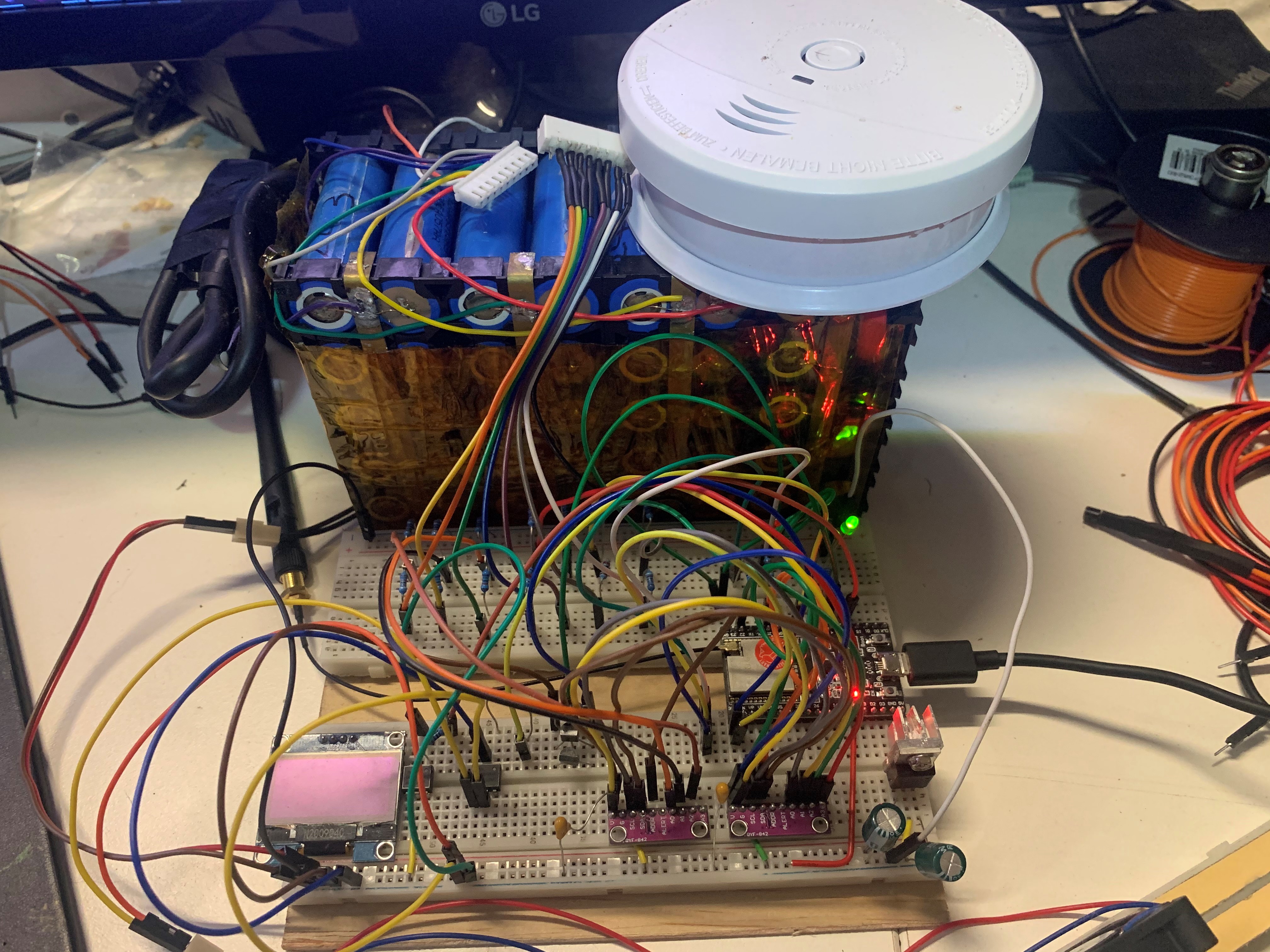
I’ve not read all of this extensive post , so apologies if this has been said ....It would be interesting to see how you’ve wired this up - hopefully not on a breadboard ?
If you were to have a bad ground connection somewhere you can easily put a high voltage into the ADS1115 and destroy it , I’d strongly suggest this is the problem area .
I would be adding some protection to the inputs ( zener diodes across input and diode upto the supply rail , maybe higher value resistors in the dividers ) to protect against that .
I wonder too if there is an issue with the timing of switching those multiplexers that results in a transient hi voltage condition on an input ( eg two inputs get shorted or are on at the same time ? Or retain charge when switching )
Finally what do the batteries drive ? Does that generate spikes in voltage ?
I'm of the opinion that using a 3.3V powered ADS1115 to measure 4.096V was doomed from the outset and a bidirectional voltage level translator should have been used to talk to the 3.3V ESP from the 5V powered ADS1115s, but that's just me. Don't let that stop you from destroying more ADS1115s. (personally, I would have tried just one , and would have posted after the second one went bad) (cost: $30)
I was curious to see how such a circuit would work in practice so I loaded in to a simulator. The schematic appears at the end:
The results for the measuring points are as follows with all cells at 4.2 volts:
V(m1): 1.89759 voltage
V(m3): 2.73913 voltage
V(m5): 2.47059 voltage
V(m7): 2.91089 voltage
V(m2): 3.30909 voltage
V(m4): 2.48182 voltage
V(m6): 2.96471 voltage
However, if I alter the voltage of one cell, the one marked V4 to 3.0 volts, it has an impact on the voltages at measuring points further up in the chain. I'm not sure how you can handle that
V(m1): 1.89759 voltage
V(m3): 2.73913 voltage
V(m5): 2.32941 voltage
V(m7): 2.79208 voltage
V(m2): 3.30909 voltage
V(m4): 2.30455 voltage
V(m6): 2.82353 voltage
Here is the complete result set for all cells back at 4.2 volts
       --- Operating Point ---

V(n001): 4.2 voltage
V(n005): 8.4 voltage
V(n002): 12.6 voltage
V(n006): 16.8 voltage
V(n003): 21 voltage
V(n007): 25.2 voltage
V(n004): 29.4 voltage
V(m1): 1.89759 voltage
V(m3): 2.73913 voltage
V(m5): 2.47059 voltage
V(m7): 2.91089 voltage
V(m2): 3.30909 voltage
V(m4): 2.48182 voltage
V(m6): 2.96471 voltage
I(R14): 0.000296471 device_current
I(R13): 0.000296471 device_current
I(R12): 0.000190909 device_current
I(R11): 0.000190909 device_current
I(R10): 0.000254545 device_current
I(R9): 0.000254545 device_current
I(R8): 0.000291089 device_current
I(R7): 0.000291089 device_current
I(R6): 0.000247059 device_current
I(R5): 0.000247059 device_current
I(R4): 0.000273913 device_current
I(R3): 0.000273913 device_current
I(R2): 0.000253012 device_current
I(R1): 0.000253012 device_current
I(V7): -0.000291089 device_current
I(V6): -0.00058756 device_current
I(V5): -0.000834619 device_current
I(V4): -0.00102553 device_current
I(V3): -0.00129944 device_current
I(V2): -0.00155399 device_current
I(V1): -0.001807 device_current
oh nice that is super cool, didnt know you could simulate stuff! So from a potential highest possible voltage I should be within boundries if I was feeding the ADS1115 with 3.3v or 5v? I handle the different voltages through some code where it works out each point in the series voltage. then subtracks the voltage from the previous and so forth. This gives correct readings for 'individual' cells. Only way I could find how to do it due to common ground being a requirement.
hammy:
I’ve not read all of this extensive post , so apologies if this has been said ....It would be interesting to see how you’ve wired this up - hopefully not on a breadboard ?
If you were to have a bad ground connection somewhere you can easily put a high voltage into the ADS1115 and destroy it , I’d strongly suggest this is the problem area .
I would be adding some protection to the inputs ( zener diodes across input and diode upto the supply rail , maybe higher value resistors in the dividers ) to protect against that .
I wonder too if there is an issue with the timing of switching those multiplexers that results in a transient hi voltage condition on an input ( eg two inputs get shorted or are on at the same time ? Or retain charge when switching )
Finally what do the batteries drive ? Does that generate spikes in voltage ?
unfortunately yes, but do i get bonus points for using 2 bread boards (see pictures)?
Having issues with ground could definitely be my issues and the more I read that the more likely it could be, was avoiding soldering it on a prototyping board before I know I have everything correct, then the plan is done with jlpcb. But I may have to test solder it all on as a final step.
From a timing perspective for the ADS being read this happens one after the other, every 2 seconds. I think I read the ADS can take up to 860ms to do a full read/convert.
These are just my test batteries on my desk, nothing is charging or being drawn of them.
By the way, I love the smoke detector in your picture. Hasn't the Boeing Dreamliner got a similar battery installation?
oh man I had no idea that you could get configured ICs that do that stuff, freaking cool. Will definitely look into that, looks like people have some guides on how they have used it and even some published PCB designs. This would be a whole new learning curve
raschemmel:
I'm of the opinion that using a 3.3V powered ADS1115 to measure 4.096V was doomed from the outset and a bidirectional voltage level translator should have been used to talk to the 3.3V ESP from the 5V powered ADS1115s, but that's just me. Don't let that stop you from destroying more ADS1115s. (personally, I would have tried just one , and would have posted after the second one went bad) (cost: $30)
All the components I have can run on 5v logic, so would it be best to have everything feed off the 5v linear voltage regulator, which provides constant/stable voltage and amps? This would make the upper limit of the ADS be 5.3v analog read be the upper limit before damage?
Don't push your luck.
You could have avoided damaging the ADC running on 3.3V by using voltage dividers that guarantee an input voltage of Vcc/2 and you didn't so from where
I am sitting , your design was marginal to begin with. This is not like coming home 15 minutes late. This is about avoiding catastrophic damage to an IC. Does the expression 'abundance of caution' mean anything to you ? Just recalculate all your
resistor values such that AT NO TIME does an analog input EXCEED Vcc/2 and you will be safe.
That's called 'worst case design' which means you design for worst case, as opposed to "how close can I cut it design' where you push all the silicon
to it's limit without mercy.
Do you really want to earn the nickname
"The Destroyer" ?
The Electron Police
Don’t go down a rabbit hole with 5V versus 3.3. Failed is failed. Start with what you have and that is failed modules. It’s a good habit to save dead things, many times they hold information in spite of being unusable. This should be one of those cases.
Has a module ever failed in the lower cell side? Or, is it always the high side unit? That would be useful information.
Hopefully, you have a DMM. Get it out. Get the failed modules. Set meter to resistance, auto range. If it’s not an auto range meter, use 2K range. Record the results, one line per module, data points left to right horizontally.
Put the black lead on the module GND. Red to VDD. Record the resistance (measurement #1).
Move the red lead to A0. Record the result. Repeat with A1,2,3, SDA and SCL. That six measurements, #2 through 7.
Move black lead to module VDD. Red to A0. Record, repeat A1,2,3,SDA and SCL. Record the six resistance measurements which will be #8 through 13.
Compare the results from say for five or six modules. That should be enough to see some patterns in the columns.
There is evidence in the failed modules. But you have to look for it.
Adding schottky diode protection to each analog input of the ADS1115 would be wise. The series
resistors should have provided good protection, but as pointed out they rely on ground being
connected reliably and before any other connections, and also rely on Vcc being always active.
MarkT:
Adding schottky diode protection to each analog input of the ADS1115 would be wise.
I agree 100%. I've used ADS1115s for years and routinely protect the inputs with Shottky diodes to both Vcc and ground. Some inputs are connected to long cable runs and there is plenty of spike-inducing lightning in my area, but I haven't lost an ADC yet despite years of continuous operation.
S.