I got JBug11 working. I can manually read and write EEPROM locations on the NMIS-0021. It might have been a change to an older FTDI adapter I found, there is mention in the docs of some adapters that can't translate a BREAK, which the bootstrap loader on the HC11 sends. I had to adjust a lot of app settings too, I'm not really sure what worked and I'm not even going to breath on it again until I can burn some working EEPROMs.
I think, both Forth and some advanced monitors, in effect do a POST diagnostic at start up, mainly to detect hardware. My theory, when it probes the EEPROM, it assumes it is RAM and abuses it until it freezes up. JBug11 doesn't even touch external memory until the port settings for that are internally enabled.
I think the EEPROM data sheet doesn't cover all the abuse cases, because after using one particular location for testing in the beginning, it now refuses to hold data while all the locations around it are fine. Today was used up just getting it to work, tomorrow I can do some more detailed investigation.
If his is in reference to https://github.com/JimInCA/motorola-6800-assembler
I finally got around to installing it, I compiled it using MinGW on Windows 11, and the resulting assembler does not have this problem. So it's a compiler bug/inconsistency of some kind, maybe?
That's very weird.
Perhaps an end-of-line issues? (ie it wants CR or CRLF at EoL, and at some point your source code switched the endings to LF? or vis versa?)
I think I tried both Unix style and the other, can’t remember now, and finally got it to work. The no blank lines thing doesn’t seem to indicate an EOL issue. It may be a OS compiler difference as I built it on a Mac or an OS specific bug. I’m used to the idiosyncrasies now.
It worked fine on the test files included which I don’t think had any 6809 ones. I just gave up and did it how it wanted. Maybe I’ll go back later and try a different compiler or OS.
I think the Moto assembler doesn't have macros. I will keep both cross assemblers around for that reason, if I didn't specify before, the other one is asxxxx from Alan Baldwin: https://shop-pdp.net/ashtml/
I haven't looked at the 6809 aspect of that, I only have time for the 6303 now. I spent some time digging deeper, and there is a warning paragraph in the HD6303Y data sheet about that.
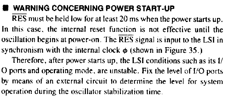
Basically it says, for that processor at least, the bus and control lines are in an indeterminate state during the required 20ms reset after power up (to allow the oscillator to stabilize). It advises you to provide protection logic for anything that has to be in a known state during that time. Luckily, I have one spare gate input on the single glue chip, that I can use to gate RAM CS* with RESET*:
This circuit can't work with the 6809, as is, because it depends on a WR* from the processor, the 6303Y is unique in having one. Normally you need to combine E and R/W* to obtain it. That would be easy, but would require an additional gate.
For anyone that's riding along, here is the decades old tried and true 68xx to static memory interface, but with the addition of a write protect input:
Is the difference perhaps due to your use of the 6809E vs. the 6809 part?
I have the Jeff Tranter SBC 6809 board working, it's running ASSIST09. I finally managed to "jailbreak" the NMIS-0021 so Forth doesn't mess with things (AFAIK it has no built in way to handle S-records anyway). https://github.com/jefftranter/6809/tree/master/sbc
My workflow now, is to cross assemble and then JBug11 loads the S-records into self contained NVRAM. That is then removed and installed in the SBC EEPROM socket. In that position, the write pin is disabled so it can not be messed with by any uploaded user programs.
I assembled the board completely stock with only three modifications - I socketed the crystal so I can experiment with different clock frequencies later on, and the reset cap is a 10uF MLCC instead of an electrolytic, and the LED current limiting resistor is changed to 10k from 330R to adjust for the LED efficiency. I did stick with red colour to maintain a modicum of retro flavour FWIW.
The workflow for the HD63C03Y will be similar, the wiring is taking a long time, there are about 30 fine wires to install, I need to set up the stereo microscope to ensure a good job on that.
I found, there are several sources of NOS HD63C03Y in surface mount, I'm really interested in what can be done with that.
Sounds like fun with the HD63 chip! Maybe there is a Schmartboard for that pin out?
On the EPROM position I separated pins 1 & 27 from Vcc so I could use A14 and *WE if I wanted to. I also disconnected RX/TX from E on the 6850 ACIA position to give me more options on where to get the clock. I also modified the crystal circuit to accept the plethora of oscillator modules I have around. Oh and changed the LED current limit to 21st century value as well.
I’m using a version of MIKBUG modified for an ACIA for old time’s sake but will change that to allow programming the EEPROM in place if wanted.
Yeah, but if you use A14 you have to sneak around the huge 8k swath of memory that repeats the ACIA registers over and over. I understand the designers dilemma... trying to keep the glue logic simple.
My thought about leaving EEPROM open to writes, too dangerous on the 8kb part because a program gone wild can sit and write it to death. It already happened to me I think. But the 32kb part has a software lock mode, you can give it a layer of protection.
I think, the ability to upload firmware is really too good to pass up. Also, 8kb is not really much ROM, unless you can use it to load more software from disk. With the board in its present incarnation, the most efficient use of memory would be to re-locate the ACIA to an expansion board, where it would have fine grained decoding to the same location, accompanied by additional memory of choice to fill the remaining space, along with any other expansion peripherals. That would increase the "unused" memory map which is available at the expansion connector, from the present 8k to almost 16k depending on the decoding. As the ACIA is mapped to 0xA000, and existing code will expect to see it there, you can only increase the contiguous RAM from 32k to 40k. But it's a start. One thing you could do, is provide 8k NVRAM disk pages from a 512 kb memory at 0x8000, additional peripherals above the ACIA in the remaining 8k. Also this would be an opportunity to buffer the expansion port, on the expansion board itself.
Yeah, I have a daughter board on the expansion connector doing more complete address decoding.
I have provided a jumper to take care of that.
The board has many shortcomings but will do for prototyping. If I recall correctly, commercial software stopped using the legacy rom monitor utility routines or provided a way to customize them in a setup program. In the 80s, 64K memory boards were available for the SWTPC, Gimix, etc. systems and they were able to accommodate decent memory maps.
I’m honing my KiCad layout skills and will end up with custom boards in the end.
Yes, by the time you do all of what I said, it's looking like there is no point having it on separate boards, you could just move everything to a single board. However I did think an expansion board for the stock unit would be neat.
As far as having boards made, it's the HD6303Y that I have my sights set on. As I discovered with the NMIS-0021 HC11 board, the more proto systems you have around, the more development options you have. Soon I will have three - the NMIS, the 6809 SBC, and whatever 6303 I can make work.
A lot of systems have jump tables to allow flexible I/O configuration at run time. If you wanted/want to over-ride a ROM function, you just replace the default vector in the table with the one you've loaded. It is not hard to make a fine grained memory map, in the past it was awkward because each additional 74LS package used board space, power, and added cost. Now all of those are much lesser.
It's not new, but easy to forget... I had it crash a few times. Started to poke around and realized USB power wasn't 5.00V, it was 4.85 and wandering up and down a few mV. So on to a proper power supply it goes...
I have a 7.3728MHz crystal, so it's just under 2MHz E clock. The symptom is, it either freezes, or starts printing garbage characters and doesn't respond to RESET (that's actually kind of unexpected). The DS1210 is configured for 4.75V standby threshold, a possible cause. I can lower it 250mV by changing the TOL input so I will try that first. If that trips, there's no memory to read.
Edit - it's been running fine for 12 hours after changing that, so there's a good chance it was the problem.
I am thinking about a Zilog Z80 having no ROM memory at all but all its memory map being implemented in SRAM; an ATMega8515 has a parallell bus interface which inherited from i8051 family but has lots of other interfaces as well.
Does anybody know about something similar to what I am describing?
The ATMega2560 also has a parallel interface, and it's brought out fully to I/O pins on the Arduino Mega. Please describe the interface you are proposing. The bus interface on the Mega is a controller, not a peripheral device like I/O or memory. So a Z80 can't "look into" the Mega. Not directly like that. There is such a thing as dual port RAM, but it's tricky.
I've seen an approach where the CPU was connected to Arduino GPIO pins, the Arduino emulates memory and I/O. But for that to work, the Arduino has to be able to halt the CPU to allow the low speed I/O to catch up.
I seems like you are talking about two different things. You can run a Z80 out of SRAM. You could program that memory with a microcontroller with a parallel bus interface. Is that what you are proposing or something different?
Question: I finally managed to program an 8k EEPROM for the Tranter board. One mystery, which plague me before, and made me wonder about almost everything, the data polling method outlined in the data sheet appears on the face of it, to not work. It is said to read bit 7 as the complement of the data you wrote, until the EEPROM write is complete. However this means that a simple test of equality should also work even though all the other bits are indeterminate. But when I coded it, it would only transfer RAM to RAM, RAM to EEPROM leaves the target unaffected. Then I gave up and simply added a way overkill 10ms wait time, and it worked! So I am left wondering what is going on...
* eemove
* 2023-03-14

* place SRAM in upper 32k
* place EEPROM in lower 32k, disconnect pin 1.
* It's duplicated four times in low memory
* Avoid the lowest page because it's in use
* Use $2000, $4000, or $6000 as base address
* for the EEPROM

source	equ	$F800
dest		equ	$5800
size		equ	$800
end		equ	source+size

		org	$8200

* make safe for debug
		psha
		pshx

* get source and target addresses into registers

		ldx	#source
		ldy	#dest

* do begin
* transfer a byte

next		ldaa	,x	A = byte
		staa	,y	move from src to dest

* Just waiting 10ms works, tested

waitpr	bsr	DLY10MS

* DATA* polling should work, but doesn't

* Do while data poll indicates write in progress
* waitpr	bsr	DLY10MS
*		cmpa	,y		byte to write is still in A
*		bne	waitpr	wait for EEPROM write complete

* Finished, point to the next location

		iny
		inx		increment pointers
		cpx	#end
		bne	next

* end while
* source pointer not at end

* wait for debug stop command

		pulx
		pula
freeze	equ *
		bra	freeze

* borrowed delay routine

DLY10MS EQU  *          ;delay 10ms at E = 2MHz
        PSHX
        LDX  #$0D06
DLYLP   DEX
        BNE  DLYLP
        PULX
        RTS

*
* end program
This is code for the NMIS-0021 running the MC68HC11A1 which has become my EEPROM burner.