I have a socket connector installed on my Tranter board for just that reason.
I will have some desoldering to do. ![]() Ah, maybe I can stack one on... that way I could even add the extra signals...
Ah, maybe I can stack one on... that way I could even add the extra signals...
2 Likes
The Tranter schematic shows a different numbering scheme in case it matters to anything you're working on.


I've been looking at a few different memory maps and thinking about how I would utilize I/O space and how much of it to leave. I'm looking at <= 32K RAM at $0 and <= 32K EEPROM at $FFFF and below.
One can easily then carve out some I/O addresses below the vectors. Lets say you want to leave $100 or $200 bytes of I/O in $20 chunks that's easily done and the rest of EEPROM can be used for code, etc.
A matrix keypad interface could be added e.g. with 2 tristate buffers. Now I know there are chips to decode keypads but you get this practically for free. Let's say you have a 4 x 8 key matrix. if you wire the "4" side to A0-A3 through a tristate buffer and the "8" side to D0-D7 through another, you can "roll" a logic HIGH down the "4" side by addressing sequential addresses that are of the nature $1001, $1002, $1004, $1008 and read the data bus to get the key pressed. One-key rollover is possible and a programmer cleverer than me could probably do more.
So anyway, I was thinking about how many locations per address would be sufficient for I/O. The Motorola family chips usually have some CS lines that could help breaking the space into more chunks if needed.
I designed a product that used the 6847 video chip and it only used $200 bytes of memory mapped character memory for a 32 x 16 alphanumeric / limited graphics display for example.
I'm in 100% agreement about the lower 32k, it should be nothing but RAM. If for no other reason than, the SWTPC and also the Searle/Tranter board, and probably most other systems have. One thing, I noticed some systems have some 128 byte RAM spaces, apart from main memory, said to be "Mikbug RAM" or something like that, in high memory. I think these were originally MC6810 RAM IC's. Is that important for a complete SWTPC emulation? Or, should those be provided via some kind of additional RAM space? I only know what I read quickly this week about the SWTPC 6809.
Can't comment on the keypad right now, just no thoughts in my head.
The VIA for example, has a ton of registers, but not 512 of them! The granularity of the address decode is usually coarser than you would like, not finer. If you're asking for an open ended opinion about that, which mostly disregards logic complexity and focuses on mapping, I would suggest for example eight 256 byte pages for I/O devices. That would occupy 2k and still leave room for additional subdivision later if more than eight selects are required. If each device is addressed at the base of each 256 byte page in software, and later more devices are needed, they could be added by decoding A7 to split those pages, yielding 8 more at the 128 byte marks between the original 8 devices (which could safely remain and operate in the original locations). This would preserve the 2k allocation for I/O, which would future proof the remaining RAM allocations.
My back of envelope designs don't currently break it down that far. As you know, there is a trade off between granularity and number of decode IC's. My focus has been to reduce the number of IC's as much as possible. I'm trying to use 138's and 139's, so the input polarities of those pull in certain directions. I try also to obtain things like ROM select from the same circuit.
I have a simple one, really it tries to align with the external address space of the Searle/Tranter board. When I get a chance, I will post KiCad examples. That one, uses one 74xx139 in cascade mode, correctly decodes four peripheral chip selects inside the 8k external ("unused") space, not including gating with E or RD* or WR*. Actually, as I mentioned, bringing RD* and WR* to the bus, means in many cases it is the only chip you would need. That is a very limited but compact decoder.
In your case, I imagine you have far more flexibility in adding more IC's to the mix. As long as you don't trespass on the external address space, you should be okay.
It's kind of unfortunate that the external space is located at $8000 since that would be the place for contiguous RAM expansion, however expansion RAM could co-exist with some peripherals in that space, with additional decoding on the expansion board itself. Also, that RAM could be an NVRAM disk, as discussed in reply #4823 (just kidding).
Regards ROM size, I personally would rather have something like a 48k/16k or even 56k/8k RAM/ROM split than a 32/32. But, a big ROM can take some pressure off the RAM if it contains software that is utilized a lot by the RAM resident programs. If you have some kind of disk, you need less ROM because you can load whatever you need.
In fact, I have been mulling over what kinds of things you could put in there. I loaded and played with Basic already, it just reminded me how much I hated it. ![]()
Yes, I wasn’t suggesting that, I was just trying to imagine what a peripheral that needed to be in the main board space would need for maximum memory. I would think that any expansion board would have its own memory if it needed a lot, a video card for example, and there would be a DMA channel from the main board if needed.
I don’t think there are any conflicts with legacy software that can’t be handled by vector tables in the ROM OS.
I’ll post my address decode scheme later when I get tired of pushing traces around. ![]()
I guess the ideal allocation would be consecutive. Not sure how it would work, kind of a blue sky distraction, but hey, position independent hardware! Back to reality and your question, I think 32 directly accessible registers is the most I've seen in a peripheral. Beyond that, they usually include some internal address register (even back then...).
I did ponder memory mapped video, it's another reason to include bus arbitration signals in the bus interface. I didn't pursue it beyond that, but there may be some interesting possibilities there.
The bus arbitration signals are key to any easy Arduino interface.
On legacy systems like the MC-10 that used the 6847, the display memory was on a separate bus from the main memory, and needed muxes and buffers to access. With that arrangement, the only time you can write the screen without glitching is during the horizontal retrace interval. Programmer has the choice to embrace or reject the glitching and run at maybe 15% speed. The memory controller on the Coco continuously interleaved CPU and video accesses to memory, making it completely transparent. I looked at DRAM to SRAM conversion and in general, it didn't look like fun. So updating that or trying to use that chip not worth the effort. But the principle works efficiently when the RAM is roughly 2 times faster than the CPU, plus a safety margin. Today, it is the address muxing that seems to be the PITA about setting that up.
Just found this
1 Like
The HD6303Y would do that well. I have been too sidetracked to work on it, but you can build a strictly three chip, no glue logic system with it and one 32k SRAM, one 32k EEPROM. The 6303Y has, in addition to onboard timer, parallel I/O, and UART, direct drive read and write signals that can be connnected directly to the memory chips without any decoding. To select between RAM and EEPROM, you can just connect processor A15 to the chip selects of both memory chips. When A15 is low, RAM is selected. When high, EEPROM is selected.
Here is the HD63C03Y board. It has 8k EEPROM, 32k SRAM, and another 32K NVRAM jumper selectable in two 16k blocks. The two bus connectors have mutual connections, a 40 pin full bus interface, and a 20 pin peripheral interface.
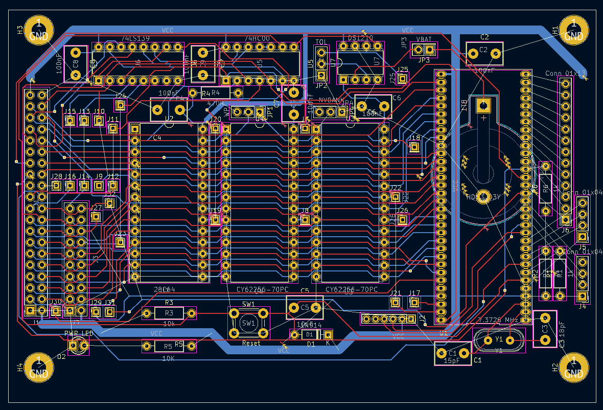
It's a double sided board, hence the numerous zero ohm resistors (wire jumpers). The ground pours haven't been done yet, after that it will go to fab.
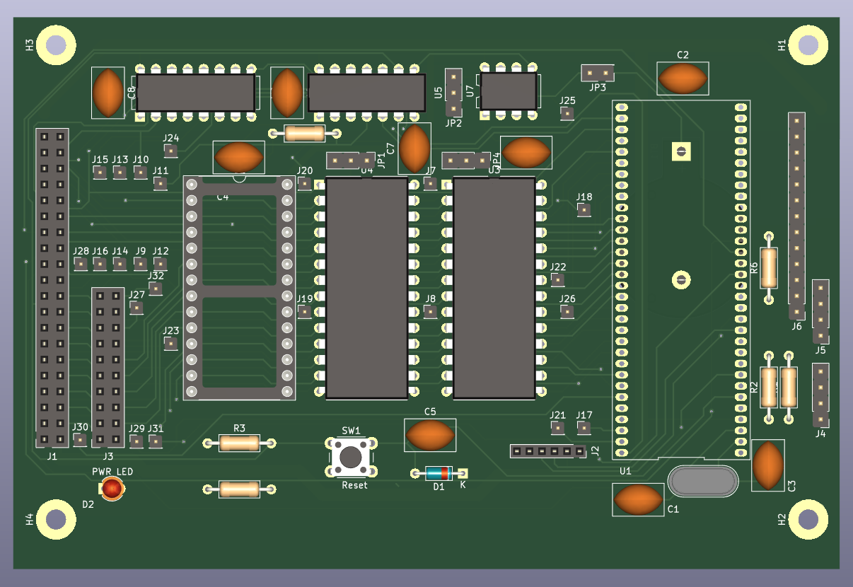
J2 will accept a USB-serial interface to provide 5V power and 115200 baud communication. The jumpers on the right hand side expose the MCU's I/O ports.
I like the looks of that! I can say that not buffering the address and data lines makes layout easier.
Yeah, it won't support much additional load on the bus connectors. Next version might have buffering... when I make a peripheral card I'll try to keep it as light as I can.
2 Likes
Wait, aren't you using #DTACK?
Instead of driving the clock directly, which is considered a dangerous practice, you should first alter your reset sequence.
Later, if you wanted other kinds of interaction the reccommended way is by the use of traps and interrupts. And of course BERR and other very useful signals that were specified for this very same purpose.
The 68k documentation can be very daunting because of his detail (and length). But if you would want to take a look into those signals, my advice would be to read this site: Motorola 68000 pins and signals.
EDIT: while #DTACK use is recommended, in your specific case it would be better to use #BR, #BG, #BACK and #HALT.
EDIT 2: I see I misread the processor and got confused. You are targetting the 6809 instead of the 68k. I could check if I can find something useful if you wanted.
As for the buffers, I would greatly recommend them. I have repaired many 8-bitters whole sole point of failure was the microprocessor, and in most cases it was not protected from incorrect connections from the outside (expansion bus) of were just overloaded. In any case, I would also advise you to read about the infamous ASICs of the Sinclair QL, where connecting or disconnecting the video output while the computer was running could kill the video circuitry.
Finally and in my opinion, I imagine most people just use pin header just because it is not known that connectors made for this same purpose exist and are still in production. If I was to design this, I would select a connector from the DIM-41612 family. Sure, they may be more expensive than pin rows, but they bring other advantages, like protecting a bit more the pins, providing a position so no accidents can occur (how many projects went to the garbage bin because human error?) and also mechanical robustness.
In any case, I hope this could be helpful to you. While having lot to learn from the AVR world and being very lame in analogic electronics, my digital logic is sound and have had experience with multiple microcomputers over twelve years.
You’re confused. This is a 6809/6309.
Yes, I noticed now. Still, there are better ways than abusing the old, poor clock. ![]()
EDIT: In that case, my advice would be to taka a look into the schematics of the Dragon Beta 128. This microcomputer is a prototype which never went into production. It has something not many micros I have seen have: two microprocessors sharing space. Usually, they may share some and under very specific circumstances (master-slave configuration). In this case they were coordinated. I saw reverse engineering schematics of it a long time ago so if you want I could take the effort to dive and search for them.
EDIT2: Went to search them anyway but links are broken. I will try to find if I had a copy of the documents saved locally.
Suggest you start a new topic.
Why? This one is not resolved and I may be able to obtain information to help all who are interested. In case I cannot find anything on my drives I still can make use of my physical technical library.
Because if you read the entire thread, you will see that it has changed to a different project. Most of the participants in this thread have the original physical data from the 70s and have been working with this microprocessor for over 45 years.
If you want to add your experience of 12 years to the mix, I suggest you start a new topic.
1 Like
I welcome any additional participation. Although the thread has veered away from the 68000 processor, I haven't completely forgotten about it. I've mainly focused on a common bus, for which the I/O bus sub-section at least, could support the 68k. Also the 6502 could be supported.
I have some answers to your comments and suggestions, which will take me some time to answer. It would be great if you could go back in the thread and try to re-interpret what you've said in the light of an 8 bit CPU.
As you probably know, the 68k can work with sufficiently fast I/O without handshaking by just grounding DTACK. There was a magazine, "DTACK Grounded" in fact.