L9780 SPI help - inconsistent output

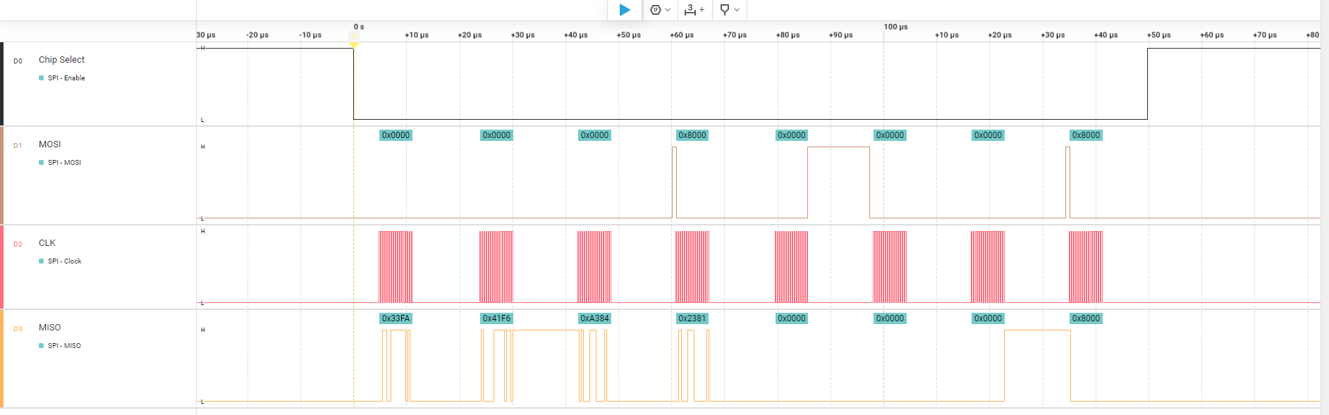
Hey all, I'm working on a program to interface with a development board I spun for an L9780 - wideband oxygen controller IC. At this point, I'm trying to get a consistent status register read back but continue to get some unexpected results that I'll explain below. This is the first "real" time I'm trying to write the SPI sequence for a chip from scratch, which is why I'd appreciate a sanity check!

The first question/verification I had was the SPI mode/setup. Searching around it looks like per the datasheet my clock is idle-low and the first data assertion (on SI) happens prior to the clock edge going high. This should correspond to a MODE0. Section 6.3 lists it as MSB first. The SPI timing table also lists 8MHz for the transfer rate; all the above should give me my config, correct?

My second question/verification was my use of the "SPI.transfer()" function. I made my way through this thread and understand the syntax behind it, so I think that part is ok.

Section 6.3.1 talks about the "REG" bit which is what's used to latch if the next SO frame contains the input reg, or the current "status" reg. This is why in my "get_status" function I'm sending out the request, and then doing another SPI.transfer (via the function) to read the result. Is this correct?

The reason I think I'm having issues is that for the status reg, the MSB is an ignored bit and then 3 version bits. Intermittently, when using my current code to test, I'm getting a change from a dec(1) value to a dec(2) value. This obviously isn't right, so while it appears I'm able to "communicate" in some form with the chip I'm guessing my formatting or byte order is FUBAR somewhere.

Is it the fact that the arduino is a little endian and I'm relating that to a SPI that transmits MSB first? From the various 64b words I've gotten back, that also doesn't appear to be the case, given the last byte also changes.

Also, per the datasheet there are some fixed (CB) bits and the SPI fault bits that should be giving some insight into the health of the current SPI frame. Both of these are giving me issues as well, which is further pointing me at that I've got something messed up with my SPI communication.

All reasons I'd appreciate some help! Below are some "outputs" from my current code just as a sample for what I'm talking about. The first few results I think are pretty well as expected from what values should be there on startup but again, I'm not 100% if what I'm getting back is "valid" anyway so...its kind of a crap-shoot.

  • SI register on startup (no setting transfer, nothing)

    • 0x4503458300C2CD31
    • 0x450345A300E26E32
    • 0x450345A300E27732
  • SI register after “send H/W config to L9780”

    • 0x370045A30002F933
    • 0x370045A30082FA33
  • status register on startup (no setting transfer, nothing)

    • 0x450345A300024632
    • Same result, multiple times
  • status register after “send H/W config to L9780”

    • 0x380045A3FFE1FA33
    • 0x380045A300E2FA33
    • 0x370045A300C2F933
  • Status register after heatup and “enable VCCS” and “enable stgINRC”

    • 0x1A031AA3001AFA33
    • 0x0C030CA3007AFA33
    • 0x1A0319A300FAFA33
    • 0x150315A3009AFA33

Datasheet:
L9780 datasheet

Current Code:

/*  Program is taken from the development firmware but simplified
 *   to menu actions for preliminary debug and troubleshooting.
 *   
 *   NOTES
 *   -------------
 *   -HTR PWM output from uC is inverse due to output FET. 15% duty
 *       applied at uC is 85% duty output from board.
 */

//*****includes
#include <SPI.h>

//*****general defines and data
#define serial_baud       9600                //serial baudrate
#define L9780_SPI_SPD           8000000                         //SPI Frequency (per L9780 timing diagram)
#define L9780_SPI_ORDR      MSBFIRST                        //define SPI order as MSB first (per L9780 timing diagram)
#define L9780_SPI_MODE      SPI_MODE0                       //define SPI mode, clock Idle LOW, first CMD sent w/o SCK (per L9780 timing diagram)
#define L9780_SO_SI       true                //used for "get status" - put the input (SI) register in SO
#define L9780_SO_STAT     false               //used for "Get status" - put the status register in SO
//pn_SPI0_MOSI              11                                  //!pinDef: SPI0 master out slave in
//pn_SPI0_MISO              12                                  //!pinDef: SPI0 master in slave out
//pn_SPI0_SCK                   13                                  //!pinDef: SPI0 clock
#define pn_L9780_CS       10                  //!pinDef: chip select for L9780
#define pn_htr_out        9                     //!pinDef: manual heater control output

//*****L9780 specific data
#define L9780_rx_reg      0x0800000000000000  //mask to get back the L9780 input register - bitOR
#define L9780_status_reg  0xF7FFFFFFFFFFFFFF  //mask to get back the status register - bitAND
#define L9780_VCCS_en     0x0040000000000000  //mask to enable operator - bitOR
#define L9780_STGINRC_en  0x0200000000000000  //mask to enable short to gnd on INRC - bitOR
#define LSU49_start_CFG   0x00040F18192A8040  //LSU 4.9 start config - non-synchronous mode
/* Config bit definitions:
 * b63-60 = 0;     not used
 * b59 = REG;      set appropriately when transmitting or receiving
 * b58 = 0;        INRC pull-down (try initially disabled)
 * b57 = 0;        INRC short to ground enable (disable on start)
 * b56 = 0;        INRC gain
 * b55 = 0;        tag resistor network switch (ch1)
 * b54 = 0;        VCCS enable (disable on start)
 * b53 = 0;        VCCS output ch (ch1)
 * b52 = 0;        VCCS pull-down (try initially disabled)
 * b51 = 0;        compensation network (chA)
 * b50 = 1;        VCCS voltage clamp enable
 * b49 = 0;        VCCS voltage clamp switch (ch1)
 * b48 = 0;        VCCS voltage clamp symetry (symetric)
 * b47 = 0;        fault clear (don't clear any faults)
 * b46-43 = 0001;  purge current (-14uA) (taken from L9780 test docs)
 * b42-40 = 111;   FV out gain (12) (taken from L9780 test docs)
 * b39-34 = 000110;VCCS capacitance (assumed Rtag ~130 ohm)
 * b33-32 = 00;    measurement clock period 4MHz
 * b31 = 0;        heater short to battery threshold (250mV)
 * b30-24 = 0011001; RCT1 switch time pulse duration (taken from L9780 test docs)
 * b23 = 0;        operation mode (free-running)
 * b22-16 = 0101010; RCT1 bandgap switch pulse duration (taken from L9780 test docs)
 * b15-14 = 10;    SPI confirmation bits - always 0b10
 * b13 = 0;        not used
 * b12-11 = 00;    heater short to battery fault time (80 Tosc)
 * b10-8 = 000;    INRC switch time pulse duration (taken from L9780 test docs)
 * b7 = 0;         protection FET ch2 (disabled)
 * b6 = 1;         protection FET ch1 (enabled)
 * b5-0 = 0;       not used
 */

void setup() {
  Serial.print(F("Initializing uC.............."));
  Serial.begin(serial_baud);          //start serial. Needed for more than just debug
  
  pinMode(pn_L9780_CS, OUTPUT);       // set the CS pin as an output
  digitalWrite(pn_L9780_CS, HIGH);    // set the CS pin to HIGH (off) 
  SPI.begin();                        // initialize the SPI -> library begin function sets output pins
  
  pinMode(pn_htr_out, OUTPUT);        // heater PWM output
  digitalWrite(pn_htr_out, HIGH);     // turn htr PWM off

  Serial.println(F("Init Complete!"));

  //****display menu
  Serial.println(F("Menu Options"));
  Serial.println(F("--------------------------------------------------------------"));
  Serial.println(F("1)  Init - Send H/W config command to L9780"));
  Serial.println(F("2)  Init - Heatup WBO2 sensor"));
  Serial.println(F("3)  L9780 - Enable VCCS (start operation)"));
  Serial.println(F("4)  L9780 - Enable stgINRC (start closed-loop L9780 control)"));
  Serial.println(F("6)  L9780 - Get status register"));  
  //****end display menu
}

void loop() {
  while (Serial.available() == false){} //wait for user input
    int menu_choice = Serial.parseInt(SKIP_ALL);  //get user input
  Serial.println(menu_choice);

  char c[150];                          //char string for menu outputs
  switch (menu_choice){
    case 1:
      L9780_SPI_xfr(LSU49_start_CFG);                   //set initial config values over SPI
      break;
    case 2:
      heatup_WB02();                                    //heat-up sequence
      break;
    case 3:
      L9780_SPI_xfr(LSU49_start_CFG | L9780_VCCS_en);   //enable VCCS (start operating)
      break;
    case 4:
      L9780_SPI_xfr(LSU49_start_CFG | L9780_STGINRC_en);//enable INRCSTG once started
      break;
    case 5:
      {uint64_t data = L9780_get_status(L9780_SO_STAT);   //get current status output
      Serial.print(F("Status Reg (64b): 0x")); SerialPrint_u64(data, true);
      }break;
    default:
      Serial.println(F("Input not recognized, please enter a valid number"));
      break;
  }
  Serial.println(F("--------------------------------------------------------------"));//bookend lines
}

/*  FUNC:   Serial Print unsigned 64b value
 *  DESC:   Fucntion prints an unsigned 64b wide value
 *  ARGS:   v   - value to print
 *          nl  - true/false to print a new line
 *  RETN:   none
 */
void SerialPrint_u64(uint64_t v, bool nl){
  char c[] = "00000000"; //temp byte to print
  sprintf(c,"%08lX", (v>>32)); Serial.print(c);
  sprintf(c,"%08lX", v); Serial.print(c);
  if(nl){Serial.println();}                         //if selected, print newline
  return;
}

/*  FUNC:   WBO2 sensor heatup
 *  DESC:   Fucntion called on sensor initialization
 *          and controlls the initial heatup cycle, including
 *          the condensation and ramp phase.
 *  ARGS:   none
 *  RETN:   none
 *  NOTES:  PWM out from L780 is inverse from arduino output
 */
void heatup_WB02(){
  Serial.println(F("-----Starting Sensor Heatup----"));
  int htr_pwm = 211;
  analogWrite(pn_htr_out, htr_pwm);                 //condensation stage
  Serial.println("---Condensation Phase");
  Serial.print("HTR PWM %: ");Serial.println(htr_pwm*20/51);
  delay(11000);                                     //simplified wait for ~20s total for condensation stage to be done
  Serial.println("---Condensation Phase End");

  htr_pwm = 76;                                     //start ramp phase, start at 70% duty (approx 8.4V)
  while(htr_pwm > 0){                               //increasing by 2/255 every 250ms is approx 0.4V/s for ramp phase 
    Serial.print("HTR PWM %: ");Serial.println(htr_pwm*20/51);
    analogWrite(pn_htr_out, htr_pwm);               //set PWM
    delay(250); htr_pwm -= 2;                       //increase/ramp
  }
  
  Serial.println(F("-----Sensor Heatup Complete----"));
  return;
}

/*  FUNC:   L9780 SPI transfer
 *  DESC:   Fucntion sends a SPI command and receives its result
 *  ARGS:   d   -   data being sent on a SPI transfer
 *  RETN:   spi_buf - data result
 *  NOTES:  Calls "begin transaction" before every send to ensure
 *                  that if another SPI library is being used that updates
 *                  these values, that they're appropriately set for L9780
 */
uint64_t L9780_SPI_xfr(uint64_t d){
  uint64_t spi_buf = d;                             //data to send
    
    //SPI transfer
    SPI.beginTransaction(SPISettings(L9780_SPI_SPD, L9780_SPI_ORDR, L9780_SPI_MODE)); //start SPI transaction
    digitalWrite(pn_L9780_CS, LOW);                                     // set the CS pin to LOW (on)
  SPI.transfer(&spi_buf,8);                         //pass address of temp data + size (8 bytes for uint64t)
    digitalWrite(pn_L9780_CS, HIGH);                                // set the CS pin to HIGH (off)
    SPI.endTransaction();                                                           //end SPI transaction
    
  return spi_buf;                                   //return rx'd data from L9780
}

/*  FUNC:   L9780 Function - Get status register
 *  DESC:   Fucntion reads the current status register
 *  ARGS:   act - true/false to select what is in SO
 *                  true - RX'd data (current SI)
 *                  false - status register 
 *  RETN:   d - SO register
 *  NOTES:  After sending data, per the datasheet the
 *          next SPI frame will have the associated data
 *          in the SO depdending on the asserted REG bit.
 */
uint64_t L9780_get_status(bool act){
  if(act = L9780_SO_SI){L9780_SPI_xfr(L9780_rx_reg);}//request input reg back
  else{L9780_SPI_xfr(L9780_status_reg);}             //request status reg back
  uint64_t d = L9780_SPI_xfr(L9780_status_reg);      //read result
  return d;
}

I had posted this elsewhere and made some updates based on that feedback. I updated my L9780_SPI_xfr function to shift in the passed 64b word into a uint16_t array and then I also shift that back out into a 64b result. I'm not sure if that's necessarily the most elegant way to do it, but now at least I'm getting expected answers (with one other change).

One other thing that I had mis-understood originally is that this particular chip doesn't really have an "ignore" command on the input register so every transmission I need to send the "control word" in addition to updating the REG bit to set what gets shifted into the SO register for the next SPI frame. After making those two changes I can request the SI register after sending a command and get the same result echo'd back.

I'm still having some issues to chase down but the actual SPI coms appear to be functional now. When requesting the status register, the SPIF1 fault bit is set, which correlates to a "SPI command data length error" when requesting the status register. The datasheet states that the expected length is [64 + n*8] bits which I'm not 100% clear on, so I need to do some more digging into that. I'm unsure if the "n*8" part is just a nomenclature thing, or if there's other bits it's expecting beyond the 64b of the control/command register and that's why I'm getting a length fault.

Hey, Jim.

I was wondering if you'd made any more progress on this? I took on a pet project and chose the L9780 controller for running an NTK sensor. I've done the hardware side of things first and now I'm getting into the programming side. The documentation hasn't been so helpful, and I've only managed to stumble on your post here and on the ST site.

I've been busy with other projects but it's still on my radar. I haven't attached a logic analyzer yet to verify my coms which is kind of the last "make sure it's all working" part I need to do yet. I'm also working on the heater PID control but have been running into issues (which is why i need to verify the data stream). Also, I'm using an LSU4.9 so some of the below may be different depending on the sensor but....most of it should be the same.

That being said, I agree the documentation leaves a few things to be desired; so I may as well summarize everything i've seen here! Hopefully this helps, maybe we can get a few people working at it. I feel like they (ST) wouldn't keep making a product if it didn't work so someone out there knows everything I just haven't found them yet.

  • For clock polarity/phase from Table 18:
    • CPOL, clock polarity = 0
      • Timing diagram shows that the clock pulses high after CSN is asserted
    • CPHA, clock phase = 0
    • The above corresponds to a MODE0.

Also, This Link to the ST forum has two supplemental PDFs for the "setup proposal" and "measures report". The "setup proposal" has some decent information in it. Some highlights:

  • Symmetrical clamping voltage on the SNS line of 2V seems to line up with other information I've found. Not sure if that applies to the NTK or not.
  • INRC short to ground should be initially disabled due to startup inrush
  • For the internal cell resistance equation:
    • R1 = RRCT21
    • R2 = RRCT22
    • Rt = RRCT1
    • R,ds_on = 9.5 ohm or can be simplified to 9ohm. This is dependent on RCT1,sw and RCT1,bg,sw. RCT1,sw is 4 to 16 ohms and RCT1,bg,sw is 2 to 16 ohm. Using the values in the R,cell calculation shows its not very dependent on R,ds_on so using the nominal value of the two (just the averaged middle value) should be OK at least for testing.

Also, I've been intermittently experimenting with if the "fault clear" command needs to be regularly sent. Ideally once things get running as expected, it shouldn't be an issue but I've been experiencing some startup faults even just during initial communication. I've noticed sending a fault clear can sometimes help, since if a fault status is detected the L9780 goes into a standby mode.

Where I'm at now is it seems I can power-up the chip, send my initial configuration word, and successfully get status back. However, to implement the PID control for the heater, I need the RCIMP1 and RCIMP2 values (*to plug into the cell resistance formula). Currently, I'm getting unexpected values (they're bot the same) so that's why I need to come back and verify that my data stream matches what I'm seeing in my terminal.

I've attached what I currently have as a "simple menu" operation that uses the terminal to send/receive commands and outputs to help troubleshooting. Also I've attached an excel workbook that has some decoding and other tools I've used when gathering information.

The idea behind the "simple menu" program was to step-through the "startup" process and check what kind of status is returned as well as being able to manually calculate the cell resistance from getting the status words, before fully implementing the PID control. The functions are in there to do it, they're just not hooked up yet. This is very much still a WIP but hopefully it helps. Once I have time to come back to this I'll update with anything I find.

L9780_simple_menu.ino (16.0 KB)
L9780_calc_tools.zip (37.7 KB)

I've been playing around with the Excel sheets you sent. It certainly seems like you've spent some time on this! I added a sensor temperature estimation "R,temp" and a few large charts based on (what I'm sure is mostly wrong beyond the OEM chart) the Temp/Resistance curve and plotted that against values a range of ADCi and ADCf values from 10-1020ADC.

It might be a close enough calculation to use for target heater control. Sadly, I can't upload anything since I just started this account.

I still can't find a single piece of OEM data for the NTK sensors so I imagine I'm going to have to buy a couple to test and hope I don't break anything.

I'm not sure that making a lookup table for the ADC,i / ADC,f values is going to gain anything (what you're talking about for the "R,temp" estimation). Since it's a two-variable equation there's no "speed" to be gained in the calculation by doing that. The equation is already in the code but I'm not currently getting expected values, which is why it's not enabled.

Also just as a second reminder, everything in that spreadsheet is set up for an LSU 4.9, not an NTK style widerange sensor; so some of the control word and other things like the resistance vs temp graphing I've done, the lambda extrapolation, etc. will likely not be applicable.

The graphing was for my own understanding purposes. I like to visualize how the variables interact as a personal matter. It's just my learning style, I suppose.

Also, I'm fully aware these sensors will not behave alike, so I'm prepared to have to do testing to find out what the NTK sensors needs. That being said, they are made of roughly the same materials, so there is reason to believe they won't be wildly different (famous last words, yeah?). They are pricey boogers so I'll be taking it cautiously when I get my PCBs.

Hello, do you have any progress on this? I have developed a system based on STM32 for L9780, however I've got a problem that RCIMP1 value is rapidly changing based on the heater duty and the value of cell resistance is floating. Additionally, even with maximum duty I can not reach 300 ohms, maybe the sensor actually needs exhaust gas to reach the operating temperature, not the heater alone?

I have tried to increase the tB time (before RCT switch is turned on) and the RCIMP1 value is more steady, but still not fully. I am thinking about implementing a digital filter, but I think that the variations are too big (e.g. randomly jumping from 1000 to 1600 ohm)

I pieced together a board in hopes to control an NTK sensor, unfortunately missed adding the FV trace from the L9780 to the STM32 on my PCB. After talking with another manufacturer, I just went with their control system so I never even got to do any actual testing of my own.

I had to run through my notes about this, but it looks like the Band Gap time (tB) is used to "recharge" the circuit between after RCIMP2 measurement. Are you running the MCP bits at their fastest measurement period ( 00 was 40k Tosc while 11 was 400k ). Maybe the circuit needs more stabilization period between measurements?

Is the RCIMP2 measurement steady and just RCIMP1 bouncy?

Yup, only the RCIMP1 bounces. I am sure that starting the heater PWM makes things worse, I have live plot of the values and a clear pattern can be seen, that indicates charging/discharging, however this does not correspond to my heater frequency nor the harmonics (period of this noise is about 150-200 ms). Tweaking the PWM frequency, clean-current value, or tB and tR times sometimes does help a bit, but I think that the measurements are shit: after increasing the duty from 70% to 100% the steady RCIMP2 goes slowly down, then if I sharply turn the heater off, the RCIMP2 goes rapidly high (so the resistance goes low)


I will call @jungle_jim also, he was also working on the topic so maybe he had done some advancements.

Oh, I forgot. I am running the slowest clock (40k Tosc). Have also tried synchronized mode with SY, to no avail.

What did you end up going with for a solution? I haven't had time to work on this among other things going on but since the last update I had made some additional notes for bench-testing. Nothing noteworthy though until I can do a logic trace.

I haven't gotten far enough to start scoping the line yet so this is outside any help i might be, sorry.

To your previous post though, the sensor should be able to reach the 300ohm range on its own without the need for exhaust gasses. Nearly every commercial solution i've used over ~20 years has no issue reading a high out of range o2 concentration (basically free-air) when the car is off and then subsequently also reading O2 when it's cranking/just started (after a warm-up period).

1 Like

I have started suspecting that my test sensor (used in a diesel BMW and maybe worn out) is just faulty. Tomorrow I will connect it to an aftermarket gauge and check, because the problems are weird.

However, I have set the MCP to 01 (state machine clock 80000 Tosc) and have got the same error as you - the same values for RCIMP1 and RCIMP2. See attached screenshot - I do not have PID yet and change the duty roughly, however after changing the duty from 30 to 40 % I suddenly got the same values. I have a scope connected to the sensor and can confirm that the RCT2 bandgap switch stopped working. Also, I have got STBS value 0x4 what corresponds to "short to battery on SR pin"

Will be exploring this in the next few days. I'll share my current control word: 0x8010fd192a8000

However I have put so many effort in this that I am starting to suspect this IC is garbage, at least because of lacking documentation and any support from ST. CJ125 is far better, considering its ease of use and how less additional components does it need. I am sure that big companies that buy it have access to better documentation.

I snagged an AFM module from ECM-Co which will just interface with my module via CAN. Seemed like an easier solution since they are well established for having good sensor control/measurement and I can switch between Bosch 4.9 and three or four different NTK sensors if ever needed.

I'm bummed I couldn't make the first unit work out.

1 Like

I have successfully obtained pump current output that is about -3,5 mA in free air and behaves appropriately when exposed to lighter flame.

Problems that I have encountered with cell resistance:

  1. I mistakenly connected the heater with incorrect polarity. Between the sensor element and the heater core, there is a parasitic capacitance - apparently the direction of current through the heater matters a lot.
  2. I mentioned earlier that I got "short to battery on SR pin" error (despite having the error-checking functionality explicitly disabled in my input word, but that's another story). Turning on PG1 (or PG2) causes the problem to disappear. The datasheet does not describe SR pin function explicitly, I wonder what impact it has on the measurements, because the pump current flows not through the SR pin, but to ground through PG's drain resistor (but the pump current will rather stay the same because it's a series connection). The "setup proposal" from ST also turns on one of the PG's. I just do not understand fully what happens here, mostly because the SR (Sensor Return?) pin looks useless, at least with its current name. Maybe the proposed value (10k) of the resistor on SR pin is too big.

I will check the lambda output against an aftermarket high-performance controller and share my results. If this works, I will implement the calculation of Rtag (Rtot) value and do serious testing with different sensors.

That's great to hear! Few things:

RE: the SR pin, that should be what's connected to the common point for the VS and IP cells on the sensor, correct? Like it states in the datasheet it's the "sensor return" line but like you said, it's not the primary current path; I suspect the name is just a little confusing and its really a "sensor return monitor" more than anything. This seems to align with what section 4.10 states (and a few other spots) and it appears to me that it's (the SR pin) only being used as a means for providing and monitoring sensor protection features.

I've got some notes on the cell resistance based on one of the accompanying STM documents, which are below. Unsure how far you've chased that so this may be redundant/superfluous to what you have but wanted to pass it on.

The "setup proposal" document has the actual equations for it, looking at the circuit it appears that:
R1 = RRCT21
R2 = RRCT22
Rt = RRCT1

ADC,i and ADC,f I'm not 100% sure on but based on the equation the "i" value that's related to the V,i pin on RCT2 but it should be the "larger" of the RCPIMP1 or RCIMP2 values. Some prelim testing I had done made me think that it should be RCIMP1 but that's when i was running into my own inconsistencies.

For R,ds_on I did a quick sensitivity in a spreadsheet just to verify the "nomninal" value. Basically since RCT1 connects through ground and then the bandgap voltage switch, there's a couple known resistances that get used for figuring out that equivalent resistance. RCT1,sw is 4-16 ohms and then RCT1,bg is 2-16. Puts the "middle" of the range around 9-10 ohm.

Just using a fixed value for ADC,i and ADC,f along with the above values to produce an ideal R,cell calculation of ~300ohms for the ideal target, I ran through the full range for R,ds on. For R,ds_on = 2ohms the calculated R,cell=295.7ohms and for R,ds_on = 16ohms the calculated R,cell = 305.3ohms.

I don't think the +/- 10ohm swing on that is going to have a whole lot of effect especially on a targeted temperature, so just using a nominal 9, 10, or 9.5 is going to be "close enough" for an acceptable calculation.

Yup, I think that you are correct - looks like the SR pin is for monitoring purposes only.

Regarding the cell resistance, I used the equation from setup proposal as well. ADCi is RCIMP1 and ADCf is RCIMP2.

About Rds_on - I have assumed a value similar to yours (9-10 ohm), but this probably does not matter at all. I have tested with different ESR targets on my PID controller that even +- 20 ohms (280 or 320) does not change the output (the Ip) of the sensor at all, so an approximation should be fine.

I am not sure I had done something wrong, but my current is inverted - page 24 of datasheet says that the VCCS current formula has minus sign, but with this sign I get inverted readings in free air (or air in my room has no oxygen, hehe) but getting rid of the sign fixes everything. Will inspect this.

I have also - probably - found why at page 5 of the "measures report" they had an error with LSU 4.9 that they had 3,45 mA pumping current. Rtot for LSU4.9 used for calculation of VCCS current is 61.9R, not 61.9R // TAG resistor, because the purpose of the TAG is to make consistent voltage drop across 61.9R. This is why with ADV their values were fine. I have done the same error at the beginning, now I get a very good reading of about 2,28 mA in open air, corresponding fully to Bosch's lookup table.

The only thing I do not understand yet is the VCCSCAP. I do not see a way to measure the TAG resistor value without developing a measurement circuit connected to mcu, or measuring it by hand. But most of the probes have resistance in the same range, so the value can be just approximated, I think.

I'll get back after testing on car.

I hadn't gotten far enough to bother with it yet but one potential option I had considered was using a free-air calibration routine to calculate the appropriate TAG resistor value to use in the various equations.

That being said, w.r.t. the correct VCCSCAP value, i think using the value from the "setup" document would be sufficient for getting something working. Also, I guess is there any good literature on a "typical" tag resistor value? I've seen anything around 130R or so. That being said, using the R,tot equation for a min/max of 100R/500R gives between 38R and 55R, which is pretty solidly around 8-9 pF for the Cint value.

Expanding that out to about 40R and 1k for the Rtag value shows (as expected) that the lower the tag resister the smaller the Cint value, which kind-of verifies that the 6pF in the setup doc as a lower bound is appropriate.

I have started to play with the L9780 and it looks like most of you are far more advanced than where I am currently. I have a PCB and I can attempt to talk to the device. From a physical hardware level, my CS, MISO, MOSI, CLK look really good and I do get some correspondence


but for some reason it seems the SPI Fault bit is always set. I am missing something obvious so hoping one of you experts may be able to assist.

I power on the device and then I send a 64bit control value (0x0000 0000 0000 8000) which is only populated with the respecitve CB1 and CB0 values.
The 64bit status returns indicates that immediately I have an SPIF issue. Find attached a screenshot of my transmission. Any help would be greatly appreciated.