Hello there!
90% of the program is already written so bear with me. I am not looking for a free ride here, just a proof-read and some pointers from the seasoned programming professionals. I am attempting to create a single phase output variable frequency square wave generator that can pass high current. I have two IGBTs mounted on a heatsink that will pulse current from a 330 V DC bus. One IGBT will handle the positive half of the square wave and the other will handle the negative. The inverter I am creating takes two 120v poles from a breaker panel and converts it to a DC bus using input diode. I have already written 90% of the program and am not looking for anybody to do my homework for me. (it's not homework it's just a hobby project) I have included pictures from the mega 2560 datasheet as well. Pin 11 needs to be High ONLY if pin 12 is Low and vis-versa. If pin 11 and pin 12 are ever high at the same time the breaker will trip. Each IGBT is rated for 400 amps because they are out of a VFD. I megged them and they meg at over 60 M ohm so they are healthy. As it stands, this program (I think) will output a square wave on both pin 11 and pin 12 but they are in phase (high as the same time and low at the same time). I need the program to trigger these pins alternately and have variable frequency. So when a potentiometer knob is turned on pin A0, both outputs will change frequency. Duty cycle needs to at or below 50%.
I really appreciate any help that any of you can give me!
I am sorry that I had to upload the program as a JPEG but the program is chock FULL of comments and supporting notes.
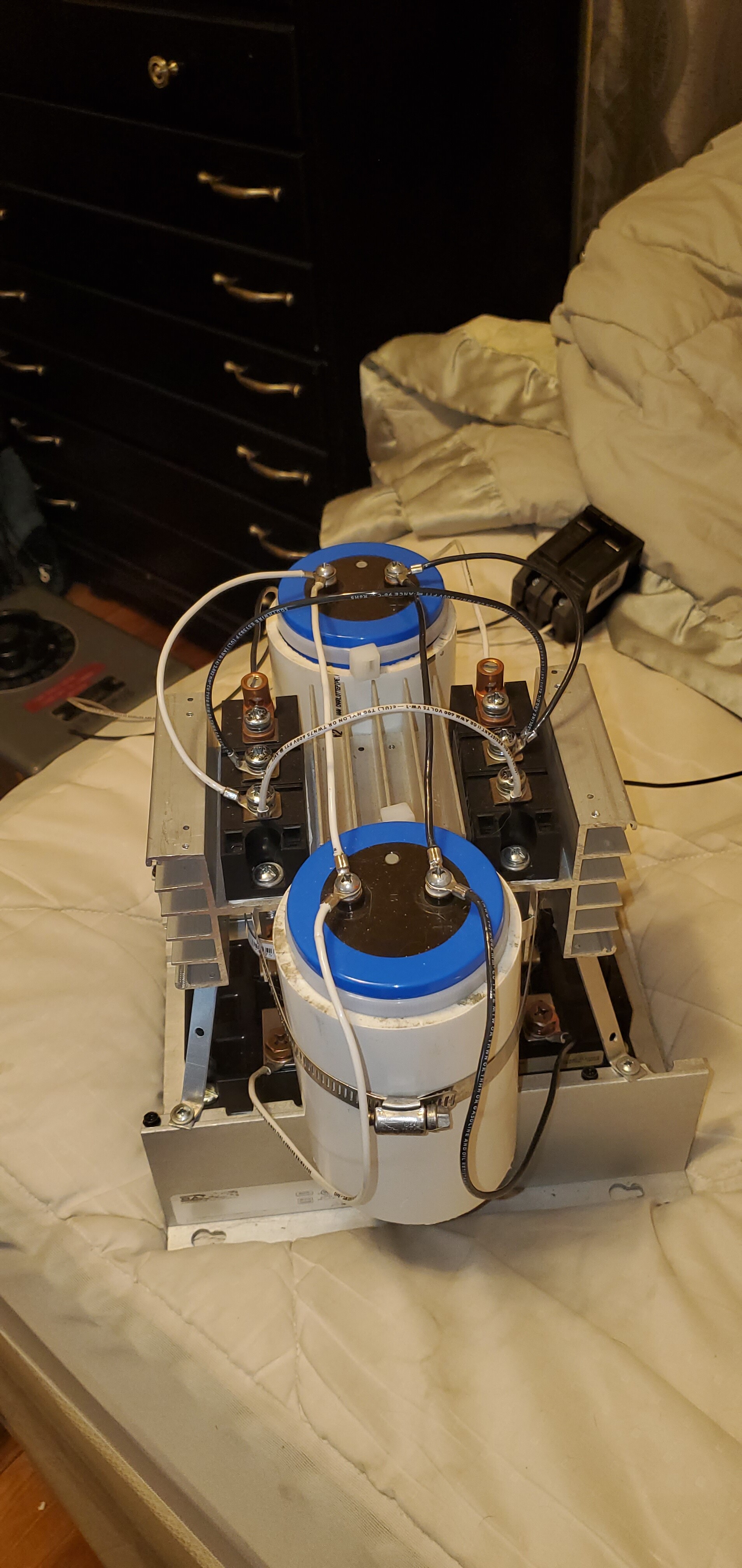
Let me know if there is a better format I can use to upload the program and I will re-do it. The picture below is of the inverter itself.
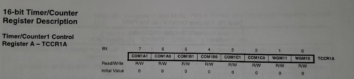
The pictures I'm uploading now are of the datasheet with timer/register/pre-scaler/bit-mode descriptions for timer1.
Can you please describe more about the waveform you want to output. Can you provide a drawing. What range of frequencies. Is the duty cycle of each output fixed?
Posting of the code images is of no use in the forum. Please read
How to Use this Forum
For 200KHz complementary pwm with deadband between the outputs, check out this thread. It may be of help. Frequency can easily be changed with a pot.
https://forum.arduino.cc/index.php?topic=438667.msg3022439#msg3022439
Be sure to put pull-down resistors on your outputs so when the processor resets and the two pins become inputs they won't accidentally float HIGH.
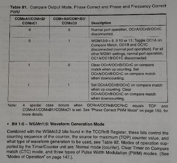
The COM1A0 and COM1B0 bits in TCCR1A should allow you to invert either of the channels. I think you will want to have OCR1A different by 1 from OCR1B to avoid the shoot-through problem.
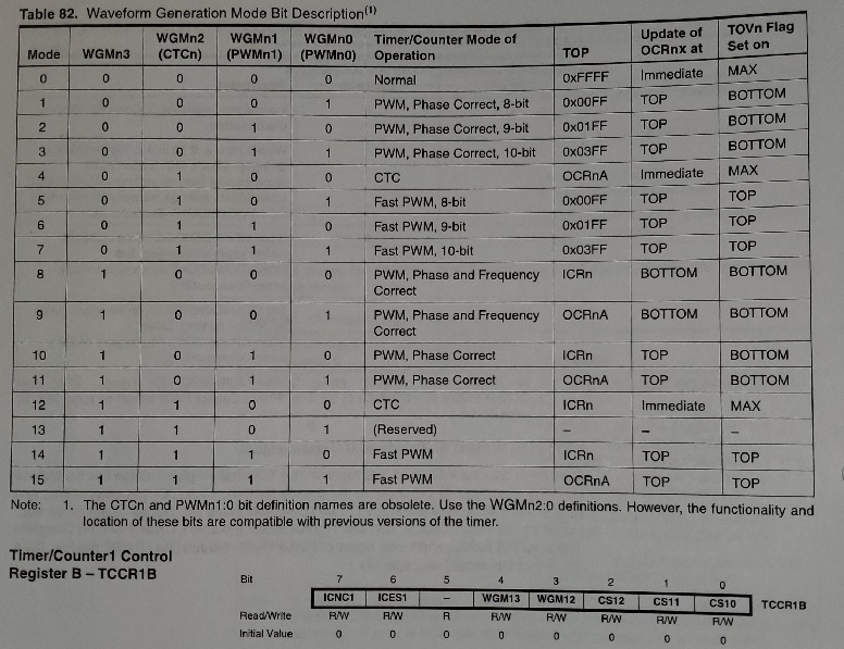
Your sketch is using WGM 9 but not using it for the PWM features! It's using a single interrupt and flipping output pins in the ISR. Since it is always flipping Pin 11 first and then Pin 12 it will cause shoot-through when Pin 11 is turning ON and Pin 12 is turning OFF. Neither pin is set to an initial state so they will likely be turning ON at the same time. SET BOTH TO 'LOW' BEFORE YOU SET THEM TO 'OUTPUT'!
I would use WGM 8 (also "Phase and Frequency Correct PWM" but with TOP in the ICR1 register). Then you can use ICR1 to set the frequency and use OCR1A and OCR1B to set the 50% duty-cycle.
Is 300 Hz the only frequency you want?
cattledog:
Can you please describe more about the waveform you want to output. Can you provide a drawing. What range of frequencies. Is the duty cycle of each output fixed?
Posting of the code images is of no use in the forum. Please read
How to Use this Forum
For 200KHz complementary pwm with deadband between the outputs, check out this thread. It may be of help. Frequency can easily be changed with a pot.
two 200kHz complementary PWM Signals - #10 by cattledog - Programming Questions - Arduino Forum
Here is a drawing with the intended outputs of both the arduino and the inverter as a whole =)
Here is the program with all the notes edited out so that it is in the correct format
#include <Wire.h>
#include <LiquidCrystal_I2C.h>
LiquidCrystal_I2C lcd(0x27,20,4);
#define IGBT1 11          //Designating pin 11 as IGBT1
#define IGBT2 12          //Designating pin 12 as IGBT2
float Freq;
int pot = A0;

void setup()

{

  pinMode(IGBT1, OUTPUT);      //sets pin 11 as an output
  pinMode(IGBT2, OUTPUT);      //sets pin 12 as an output
  lcd.init();                            //start lcd serial communication
  lcd.backlight();                    //start lcd backlight
  lcd.clear();                         //clear lcd display
  delay(1000);                       //delay of 1000 milliseconds
  noInterrupts();                    //disable interrupts
  TCCR1A = 0;                       //Initialize entire timer 1 register A to 0
  TCCR1B = 0;                       //Initialize entire timer 1 register B to 0
  TCNT1 = 0;                        //initialize counter value to 0
  OCR1A = 52;                       //compare match register value 16MHz/1024(which is TCCR1B CS12 and CS10 below)/300Hz desired = 52
  TCCR1A |= (1 << WGM10);    //Waveform Generation Mode 9
  TCCR1A |= (1 << COM1A1);   //Set OC1A/OC1B/OC1C on compare match when upcount and clear OC1A/OC1B/OC1C when downcount
  TCCR1A |= (1 << COM1A0);   //Set OC1A/OC1B/OC1C on compare match when upcount and clear OC1A/OC1B/OC1C when downcount
  TCCR1B |= (1 << WGM13);           //Waveform Generation Mode 9
  TCCR1B |= (1 << CS12);            //Clock select bits for 1024 prescaler
  TCCR1B |= (1 << CS10);            //Clock select bits for 1024 prescaler
  TIMSK1 |= (1 << OCIE1A);          //Enable timer compare interrrupt
  interrupts();

}

 ISR(TIMER1_COMPA_vect)           //Interrupt service routine for triggering outputs

{

  digitalWrite(IGBT1, digitalRead(IGBT1) ^ 1);   //toggles IGBT1 pin
  digitalWrite(IGBT2, digitalRead(IGBT2) ^ 1);   //toggles IGBT2 pin

}


void loop()
{
  analogRead(A0, pot);
  lcd.setCursor(0, 0);
  lcd.print("Single Phase");
  lcd.setCursor(0, 1);
  lcd.print("VFD");
  lcd.setCursor(0, 2);
  lcd.print("Freq = ?");

}
johnwasser:
Be sure to put pull-down resistors on your outputs so when the processor resets and the two pins become inputs they won't accidentally float HIGH.
The COM1A0 and COM1B0 bits in TCCR1A should allow you to invert either of the channels. I think you will want to have OCR1A different by 1 from OCR1B to avoid the shoot-through problem.
Your sketch is using WGM 9 but not using it for the PWM features! It's using a single interrupt and flipping output pins in the ISR. Since it is always flipping Pin 11 first and then Pin 12 it will cause shoot-through when Pin 11 is turning ON and Pin 12 is turning OFF. Neither pin is set to an initial state so they will likely be turning ON at the same time. SET BOTH TO 'LOW' BEFORE YOU SET THEM TO 'OUTPUT'!
I would use WGM 8 (also "Phase and Frequency Correct PWM" but with TOP in the ICR1 register). Then you can use ICR1 to set the frequency and use OCR1A and OCR1B to set the 50% duty-cycle.
Is 300 Hz the only frequency you want?
Thank You! Thank You! Thank You! I was really uncertain about the WGM mode and whether I had set it and the COM bits correctly. I need the output frequency of both of the pin 11 and pin 12 outputs to change in tandem when the potentiometer knob is turned. Ideally I would have an output frequency range of between 10 Hz and about 10 kHz and both outputs would have a duty cycle of 50%
Can anybody tell me how I would set both outputs to a duty cycle of 50%? As far as adding variable frequency goes I need to use the map function on analog input A0 and use it to adjust the compare match register value right?
As far as adding variable frequency goes I need to use the map function on analog input A0 and use it to adjust the compare match register value right?
No in the mode8 you are planning to use, the frequency is set by ICR1 which is used as the top value.
Can anybody tell me how I would set both outputs to a duty cycle of 50%?
Duty cycle will be controlled by the OCR1A and OCR1B values. For 50% they will be ICR1/2. You want to have them different by one count to avoid any possible overlap.
The non overlap depends on how the COM1Ax and COM1Bx settings are configured. You want one output to be set rising and clear falling, and the other to be clear rising and set falling.
Do you have a scope to work with to help verify you outputs?
cattledog:
No in the mode8 you are planning to use, the frequency is set by ICR1 which is used as the top value.
Duty cycle will be controlled by the OCR1A and OCR1B values. For 50% they will be ICR1/2. You want to have them different by one count to avoid any possible overlap.
The non overlap depends on how the COM1Ax and COM1Bx settings are configured. You want one output to be set rising and clear falling, and the other to be clear rising and set falling.
Do you have a scope to work with to help verify you outputs?
-Oh so it's the ICR1 and ICR2 value that I have to vary for frequency.
-So different by one means output compare register values for A and B have to be OCR1A = 52 and OCR1B = 53?
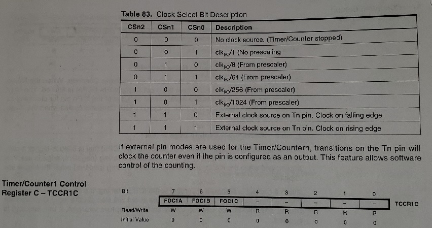
-For COM bits it gets a bit confusing for me. According to the image I uploaded earlier (table 81 in picture 20200531_041911) I have COMnA1/COMnB/COMnC1 in the first column and COMnA0/COMnB0/COMnC0 in the second column. So do I choose the fourth row in that table and set COM1A1 to 1 and COM1B to 1? Its confusing to me because it looks like its referring to Timer 0 with the zero that follows each com bit separated by a backslash in the second column. Ive spent too many nights staying up until 4 am staring at my screen trying to figure this out and googling everything, It gets my head spinning.
-Yes I have an old Tektronix TDS540A. Made the same year I was born!
-Since I am a beginner to programming the Arduino this is quite an endeavor for me. I am thankful that once I get this program running I can reverse engineer how the working program operates to gain a better understanding of how these processes are carried out.
Thank you once again for helping me. Clicking the karma button next to your name is the least I can do but it feels like I'm giving you pocket lint in exchange for gold here!
Oh so it's the ICR1 and ICR2 value that I have to vary for frequency.
ICR1 value to set the frequency. ICR2 refers to Timer2 and is not relevant to this application.
For a good tutorial on timers, read Nick Gammon's Gammon Forum : Electronics : Microprocessors : Timers and counters
For COM bits it gets a bit confusing for me. According to the image I uploaded earlier (table 81 in picture 20200531_041911) I have COMnA1/COMnB/COMnC1 in the first column and COMnA0/COMnB0/COMnC0 in the second column. So do I choose the fourth row in that table and set COM1A1 to 1 and COM1B to 1?
I don't have a data sheet in front of me just now, but I believe that with bits set in COM1A1 and COM1A0 output A set on the rising count and cleared falling count.
With a bits set in COM1B1 output B will clear on the rising count and set on falling count.
The double sloped (count up and then count down) timer modes take some extra thought. 
Here is an example I just wrote that covers 1 Hz to over 65 kHz. I have not dragged out an oscilloscope yet to verify the output signal but it measures as I would expect on my multimeter (2.5V AC from Pin 9 or Pin 10 to Ground, 5V AC betwen Pin 9 and Pin 10).
// Generating Two 180° Out of Phase Variable-Frequency Square Waves on Timer1 of an Arduino UNO (Pins 9 and 10)
// Good for integer frequencies from 1 Hz to 65535 Hz.
// Written June 1st, 2020 by John Wasser


void TwoPhaseBegin()
{
  digitalWrite(9, LOW);
  pinMode(9, OUTPUT);
  digitalWrite(10, LOW);
  pinMode(10, OUTPUT);


  // Stop Timer/Counter1
  TCCR1A = 0;  // Timer/Counter1 Control Register A
  TCCR1B = 0;  // Timer/Counter1 Control Register B
  TIMSK1 = 0;   // Timer/Counter1 Interrupt Mask Register


  // Set Timer/Counter1 to Waveform Generation Mode 8: Phase and Frequency correct PWM with TOP set by ICR1
  TCCR1B |= (1 << WGM13);  // WGM=8
  TCCR1A |= (1 << COM1A1);  // Normal PWM on Pin 9
  TCCR1A |= (1 << COM1B1) | (1 << COM1B0); // Inverted PWM on Pin 10


  TwoPhaseFrequency(1000);  // Default to 1 kHz
}


//  Will return 'false' if the frequency can't be acheived with Timer1 but it currently
// works with all values that will fit in a uint16_t so it should never return false.  For
// non-integer frequencies the argument can be changed to 'float' and then some
//  frequencies might not be reachable.
bool TwoPhaseFrequency(uint16_t frequency)
{
  byte prescaleBits; // 1, 2, 3, 4, 5
  uint16_t prescaleFactor;  // 1, 8, 64, 256, 1024
  uint32_t top32;


  // Find the smallest prescale factor that will fit the TOP value within 16 bits.
  // frequency = F_CPU / (2 * prescale *  TOP)
  // TOP = F_CPU / (2UL * prescale * frequency);

  prescaleBits = 1;
  prescaleFactor = 1;  // Used for 123-65535 Hz
  top32 = F_CPU / (2UL * prescaleFactor * frequency);
  if (top32 > 65535UL) // Too many clocks to count in 16 bits?
  {
    prescaleBits = 2;
    prescaleFactor = 8;  // Used for 16-122 Hz
    top32 = F_CPU / (2UL * prescaleFactor * frequency);
    if (top32 > 65535UL) // Too many clocks to count in 16 bits?
    {
      prescaleBits = 3;
      prescaleFactor = 64;  // Used for 2-15 Hz
      top32 = F_CPU / (2UL * prescaleFactor * frequency);
      if (top32 > 65535UL) // Too many clocks to count in 16 bits?
      {
        prescaleBits = 4;
        prescaleFactor = 256; // Only used for 1 Hz
        top32 = F_CPU / (2UL * prescaleFactor * frequency);
        if (top32 > 65535UL) // Too many clocks to count in 16 bits?
        {
          prescaleBits = 5;
          prescaleFactor = 1024;
          top32 = F_CPU / (2UL * prescaleFactor * frequency);
          if (top32 > 65535UL) // Too many clocks to count in 16 bits?
          {
            return false;
          }
        }
      }
    }
  }


//  Serial.print("Freq: ");
//  Serial.print(frequency);
//  Serial.print(" prescale: ");
//  Serial.print(prescaleFactor);
//  Serial.print(" TOP: ");
//  Serial.println(top32);


  if (top32 < 16)
    return false; // Require at least 16 levels of PWM


  TCCR1B &= ~((1 << CS12) | (1 << CS11) | (1 << CS10)); // Clear the three clock select bits
  TCCR1B |= prescaleBits; // Set clock prescale to prescaleBits


  ICR1 = top32;  // This (along with prescale) sets the frequency
  OCR1A = top32 / 2;  // 50% duty cycle, truncated, for the non-inverted wave
  OCR1B = (top32 / 2) + 1;  // Slightly less duty cycle for the inverted wave to prevent overlap
  return true;
}


void setup()
{
  Serial.begin(115200);


  TwoPhaseBegin();  // Start output at 1000 Hz
}


void loop()
{
    // Call TwoPhaseFrequency(uint16_t frequency) any time to change the output frequency
}
// Set Timer/Counter1 to Waveform Generation Mode 8: Phase and Frequency correct PWM with TOP set by ICR1
  TCCR1B |= (1 << WGM13);  // WGM=8
  TCCR1A |= (1 << COM1A1);  // Normal PWM on Pin 9
  TCCR1A |= (1 << COM1B1) | (1 << COM1B0); // Inverted PWM on Pin 10
The nomenclature of "normal" and "inverted" comes from the fast pwm or single sloped timer modes. "Normal" sets at bottom and clears on a compare match so for a 75% duty cycle, the clear match is at the top end and the output is on more than off. "Inverted" is the reverse.
For the dual sloped timer modes where the timer counts up and down with each cycle, its my opinion that the previous nomenclature is confusing. The data sheet uses
Clear OC1A/OC1B on compare match when up-counting. Set
OC1A/OC1B on compare match when down counting. (Output control bits set 1 0)
Set OC1A/OC1B on compare match when up-counting. Clear
OC1A/OC1B on compare match when down counting (Output control bits set 1 1)
I think that conceptualizing the dual sloped behavior in the data sheet terms helps to visualize the output separation and dead band generation.
cattledog:
I think that conceptualizing the dual sloped behavior in the data sheet terms helps to visualize the output separation and dead band generation.
Or we could call them 'valleys' and 'peaks' instead of 'normal' and 'inverted'. The "valleys" signal is on when the count is at or below OCR1A and the "peaks" signal is on when the count is at or above "OCR1B".
Hahaha and here I was trying to figure out how I was going to use map function to map potentiometer input on A0 to a range that I could use to control the ICR1 value. Like I was walking around with my pants on backwards.
I genuinely would not have thought to use unsigned integers for the prescale factor or the ICR register value. You have been incredibly helpfull ! The information you both have provided me with here will be commutable to future projects and I thank you for that.
Note: If "frequency" is changed from 'uint16_t' to 'float' the frequency range will be about 0.12 Hz to 500 kHz.