How to create four high frequency PWM signals with high accuracy?

Hello again.

So, I want to create four PWM square wave signals outputted from pins 11, 10, 6, and 5. Since they need to be high frequency with high accuracy to said frequency (ideally accurate up to at least the standard limit of ~62.5 kHz; more is better, though, if possible), digitalWrite and other related functions are out of the question, meaning some port manipulation is needed. However, I am fairly unknowledgeable on this topic, so I would appreciate some help.

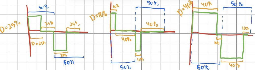
Note that the four signals are slightly different. The signals from pins 11 and 6 are the inverse of each other, and the signals from pins 10 and 5 are the inverse of each other. All signals have a duty cycle of 50%, BUT the time that signals 10 and 5 first change is time shifted depending on the desired output duty cycle (dutyCycles variable, which is the amount of time that the output signal is on positively or negatively in the half-cycle). Hence, the port manipulation code must take into account the dutyCycles variable to adjust the timing, and hopefully be adaptable to accepting a changing value of dutyCycles in future implementations. Right now, though, I just want to get this working for a constant value of dutyCycles.

Also, the formulas calculating the delays are as they are since onDelay is the amount of time the output signal is positive and negative in its two half-cycles, and offDelay is just the remaining half-cycle time. The output signal is the same frequency as the other four signals, and it is not in the code as these four signals are the control signals for an external circuit that creates the output signal.

Hopefully all of that made sense. Below is my current code. How can I make this faster. I imagine it may involve timers and/or removing delayMicroseconds, but I do not know how to properly do that.

Any help would be greatly appreciated. Thank you!

Let me know if any other information is needed.

int InvPin1 = 11;
int InvPin2 = 10;
int InvPin3 = 6;
int InvPin4 = 5;

float dutyCycles = 75;

const float frequency = 5000;
const float period = 1/frequency;

float onDelay = 0;
float offDelay = 0;

void setup() {
 
  DDRB = B00001100;                                           // Pins 11 and 10 set as Output
  DDRD = B01100000;                                           // Pins 6 and 5 set as Output

  onDelay = ((dutyCycles/100) * (period/2)) * 1000000;        // Amount of time the Positive and Negative regions on
  offDelay = (1 - (dutyCycles/100)) * (period/2) * 1000000;   // Amount of time the Positive and Negative regions off
  
}

void loop() {
  while(true) {
    PORTB = B00001000;            // Pin 11 on; Pin 10 off
    PORTD = B00100000;            // Pin 6 off; Pin 5 on
    delayMicroseconds(onDelay);   // State remains this way for 'onDelay' us
    
    PORTB = B00001100;            // Pin 11 on; Pin 10 on
    PORTD = B00000000;            // Pin 6 off; Pin 5 off
    delayMicroseconds(offDelay);  // State remains this way for 'offDelay' us
    
    PORTB = B00000100;            // Pin 11 off; Pin 10 on
    PORTD = B01000000;            // Pin 6 on; Pin 5 off
    delayMicroseconds(onDelay);   // State remains this way for 'onDelay' us
    
    PORTB = B00000000;            // Pin 11 off; Pin 10 off
    PORTD = B01100000;            // Pin 6 on; Pin 5 on
    delayMicroseconds(offDelay);  // State remains this way for 'offDelay' us
  }
}

Remember millis( ) uses interrupts, at which time your signals may get lengthened.

Using (AVR) counters the pulses can be inverted, delayed or have (non-)overlap. For high accuracy a Mega (16+16 bit) should be preferred over the Uno (8+16 bit)

1 Like

Below the link with example of generate two 200 KHz complimentary PWM signals on Uno:

2 Likes

You should draw a timing-diagram take a smartphone picture of the timing-diagram and then post the timing-diagram

how many bits written as a number means resolution with "high accuracy"?

what frequency written as a number ..... kHz would you wish ideally?

Absolutely, I should have done that previously. Hopefully the attached diagram makes clear the function of this program.

What I mean by "high accuracy" is that if the frequency is given to be 8 kHz, the output signal will be 8 kHz as well, not less than 8 kHz. To put it as a number, within 50 Hz of the host frequency would be ideal. Right now, if I enter in 5 kHz, the output frequency is approximately 4.6 kHz, and if I enter in 10 kHz, the output frequency is approximately 8.5 kHz.

The highest frequency for which I would like my program to remain accurate (within that 50 Hz range of the given frequency) is 10 kHz.

Hopefully this answers your questions. Let me know if you have any ideas.

Most probably this difference results from a resonator of deviant frequency. Calibrate your code accordingly.

you posted a timing diagram.

Still not everything clear.
You have drawn 8 parts in your diagram.
These parts show a signal with three levels

Any microcontroller can only create a two-level signal HIGH and LOW on digital IO-pins and that's it.

You have added output created by external circuitry which is post-arduino.
You haven't specified which part of the diagram shows the arduino-output
without very clearly marking
THIS part of the diagramS show the arduino output 1

THIS part of the diagramS show the arduino output 2

THIS part of the diagramS show the arduino output 3

THIS part of the diagramS show the arduino output 4

it is impossible to understand what you really want.

So please add timing diagrams that show
TWO-levels and write which diagram is what IO-pin of the arduino

I could do assumings. But I DON'T do it.


I apologize if my previous picture wasn't clear. But the signals generated by the Arduino are indeed two-level. In the previous pictures, the Arduino signals were labeled by their variable names (InvPin1, InvPin2, InvPin3, and InvPin4) just as in the code I shared originally. In this picture, I will use their actual pin numbers if that makes it more clear.

Note that the three other waveforms you highlighted were of further examples of the Output signal across the Load of differing "dutyCycles" values (D = 25, D = 10, and D = 40). I included them to showcase what the code was really affecting and why "dutyCycles" and "frequency" were variables to be concerned about. In retrospect, I realize those are slightly wrong anyway, so those should be ignored as "dutyCycles" can be between (0, 100), non-inclusive.

Again, I want the frequency of the Output signal (the signal across the Load in the diagram) to be as accurate as possible to the frequency value given in the code (see previous reply for understanding what I mean by "accurate"). This means that the frequencies of the four signals generated by the Arduino (in pins 11, 10, 6, and 5) should also be of accurate frequency.

So, in other words, what I want is for the frequency of the four signals generated by the Arduino (pins 11, 10, 6, and 5) to match the value of the frequency variable given in the code. Additionally, I would like for the frequencies of the signals to remain accurate for up to 10 kHz, meaning if I change the value of the frequency variable to 10000, the frequencies of the signals generated will be as close to 10 kHz as possible.

Is this more clear?

I apologize if this may be a dumb question, but what do you mean by this? Is there a code change or a hardware change to make?

Some microcontroller-boards use a so called resonator to create the Clock-signal.
These resonators are build to create a certain frequency but different resonators vary in their real frequency they create.
And this created frequency changes with temperature.

Some other microcontroller-boards use a chrystal. chrystals are known to be more accurately across different temperatures and to be more accurate at all.

So a different microcontroller-board with at least a chrystal instead of a resonator
a different chip that can be used with chrystal and a higher clock-frequency will be more precise.

If you want to keep the microcontroller-board you will have to write a translation-table
which uses the real frequency as input and sets the software-parameters to a value which results in the exact frequency.

Example
You want to have 5 kHz. But your microcontroller creates 4.6 kHz
this means you have to change the parameters to a higher frequency

  • just as example-number to demonstrate the principle -

you set frequency to 5.73 kHz to obtain a defacto real frequency of 4.95 kHz
which is in your range of 50 Hz precision

You might be able to tweak it some more by setting the frequency to 5.76 kHz to obtain a defacto real frequency of 5.01 kHz

Isn't the cheap resonator in an Arduino Uno rated for 0.5% precision? So 5000+/-25Hz? Or 10000+/-50Hz?

The OP code is likely slow due to the 4 sequential delayMicrosecond() errors accumulating:

If one didn't want to figure out the hardware timers, and do it in software as in the original post, one could use a if(micros() - last ....) trick to average out the errors instead of accumulating them.

Maybe replace your final delay with a variable error-absorbing delay like:

  //    delayMicroseconds(offDelay);  // State remains this way for 'offDelay' us
  while (micros() - last < 1000000 * period) {
    ;
  }
  last += 1000000 * period;
  }

Try the OP's code (and this change) in the UnoScope - Wokwi ESP32, STM32, Arduino Simulator

You should develop the habit of writing the real numbers NEW instead of pointing "foggy" to other postings.

So with writing the real numbers NEW your text would look like this

I want
if the frequency that is used as the input-number is 5 kHz
I want the frequency that is really created on the Output to be as accurate as possible to be 5 kHz too.
The maximum deviation from the ideal frequency shall be 50 Hz.

As an example:
Code uses 5000 Hz as the "input-number" for frequency
the real created output-frequency should be in the range of 4950 Hz to 5050 Hz
= 5000 Hz +- 50 Hz.

Then everything can be read in this one actual posting instead of searching through a lot of postings to collect the details.

This reduces the effort for your (potential) helpers a lot.
You should re-read your posting after writing two or three times and check:

Is all relevant information in it? You should insert postings that describe functional details as a link to make it easy to access them for readers

Example: The timing diagram posted in post # 9

Shows how IO-pins 5,6,10,11 shall be switched HIGH/LOW

1 Like

1. Generation of 5 kHz PWM signals on the following DPins (Fig-1) of ATmega328P mCU of the Arduino UNO Board.
pwm328-1
Figure-1:

2.
DPin-9: Non-invert PWM signal using TC1 in Mode-14 (Fig-2)
DPin-10: Inverted PWM signal using TC1 in Mode-14 (Fig-2)

Duty cycles of both signals can be changed simultaneously by rotating R1-pot (Fig-1)

Sketch:

#define OC1A 9
#define OC1B 10

void setup()
{
  Serial.begin(9600);
  pinMode(OC1A, OUTPUT); //Ch-A
  pinMode(OC1B, OUTPUT); //Ch-B

  TCCR1A = 0x00;   //reset
  TCCR1B = 0x00;   //TC1 reset and OFF
  //fOC1A = clckSys/(N*(1+ICR1)); Mode-14 FPWM; OCR1A/OCR1B controls duty cycle of Ch-A/Ch-B
  // 5 kHz = 16000000/(8*(1+ICR1)) ==> ICR1 = 399, N = 8

  TCCR1A |= (1 << COM1A1) | (0 << COM1A0);  //Ch-A non-inverting, Mode-14
  TCCR1A |= (1 << COM1B1) | (1 << COM1B0); //Ch-B inverting
  TCCR1A |= (1 << WGM11);
  TCCR1B |= (1 << WGM13) | (1 << WGM12); //Mode-14 Fast PWM
  ICR1 = 399;  //changes frequency as ICR changes
  OCR1A = 200;   //~= 50% duty cycle; Ch-A
  OCR1B = 200;    //~= 50% duty cycle Ch-B
  TCCR1B |= (1 << CS11); //N = 8   //Start TC1 with division factor 8
  delay(200);
}

void loop()
{
  OCR1A = map(analogRead(A0), 0, 1023, 40, 360); //duty cycle: 10% to 90%
  OCR1B = map(analogRead(A0), 0, 1023, 360, 40); //duty cycle: 90% to 10% 
  delay(200);
}

3. Possible Waveform Modes of ATmega328P MCU

tccr1a


Fifure-2:

4.
DPin-11: Non-invert PWM signal using TC2 in Mode-5 (Fig-2)
DPin-3: Inverted PWM signal using TC2 in Mode-5 (Fig-2)

Duty cycles of both signals can be changed simultaneously by rotating R1-pot (Fig-1)

Sketch:
Left as an exercise for the OP.

This part of your timing-diagram shows the output-signal which will be created through your external circuitry.
Your outputsignal has three voltage-levels:

shows
how the Arduino IO-pins 5, 6, 10, 11 which are feeded into your 3-level external-signal-circuitry
are switched LOW/HIGH.

This picture shows it for timing-intervals that are exact 25% of the output-period.

How do the Arduino IO-pins 5, 6, 10, 11 signals look like for this 3-level-output-signal?


additionally:

trying to be fast slows things down:
maximise your support by supporting your supporters
you are the one who wants help.
You should take the effort to describe the wanted functionality in an easy to understand way.

The easier it is to understand what you want the more users will contribute.

Write all letters and numbers with an amount of precision that they are easy to read
As you have written in in the picture above it needs very careful looking and logic conclusions
which might be wrong to read your numbers.

How do the Arduino IO-pins 5, 6, 10, 11 signals look like for this 3-level-output-signal?

Your 3-level-signal is no longer a classical PWM-signal.
So it doesn't make sence to talk about a "duty"-cycle
Without the picture everybody else than you would be totally lost about the meaning
So very good that you posted this picture.

@GolamMostafa
I took your code

#define OC1A 9
#define OC1B 10

void setup() {
  Serial.begin(115200);
  Serial.println("Setup-Start");
  pinMode(OC1A, OUTPUT); //Ch-A
  pinMode(OC1B, OUTPUT); //Ch-B

  TCCR1A = 0x00;   //reset
  TCCR1B = 0x00;   //TC1 reset and OFF
  //fOC1A = clckSys/(N*(1+ICR1)); Mode-14 FPWM; OCR1A/OCR1B controls duty cycle of Ch-A/Ch-B
  // 5 kHz = 16000000/(8*(1+ICR1)) ==> ICR1 = 399, N = 8

  TCCR1A |= (1 << COM1A1) | (0 << COM1A0);  //Ch-A non-inverting, Mode-14
  TCCR1A |= (1 << COM1B1) | (1 << COM1B0); //Ch-B inverting
  TCCR1A |= (1 << WGM11);
  TCCR1B |= (1 << WGM13) | (1 << WGM12); //Mode-14 Fast PWM
  ICR1 = 399;  // changes frequency as ICR changes
  OCR1A = 200; //~= 50% duty cycle; Ch-A
  OCR1B = 200; //~= 50% duty cycle Ch-B
  TCCR1B |= (1 << CS11); //N = 8   //Start TC1 with division factor 8
  delay(200);
}


void loop() {
  OCR1A = map(analogRead(A0), 0, 1023, 40, 360); //duty cycle: 10% to 90%
  OCR1B = map(analogRead(A0), 0, 1023, 360, 40); //duty cycle: 90% to 10% 
  delay(200);
}

flashed into an arduino uno and scoped the signals of IO-pin D9 / D10
This is what it looks like


D10 is shifted behind D9 but the ON/OFF times are the same.
I guess this is not what the TO wants.

Please, comment out two lines in the loop() function of post #14 and then scope at DPin-9; a 5 kHz wave close to 50% duty cycle should appear. After that hook up another scope probe at DPin-10 and trigger properly against Ch-A/internal; an inverted signal should appear. If not, please report to allow me investigating the possible flaw in the codes of post #14.

This the code with the two lines with call to map-function commented out

#define OC1A 9
#define OC1B 10

void setup() {
  Serial.begin(115200);
  Serial.println("Setup-Start");
  pinMode(OC1A, OUTPUT); //Ch-A
  pinMode(OC1B, OUTPUT); //Ch-B

  TCCR1A = 0x00;   //reset
  TCCR1B = 0x00;   //TC1 reset and OFF
  //fOC1A = clckSys/(N*(1+ICR1)); Mode-14 FPWM; OCR1A/OCR1B controls duty cycle of Ch-A/Ch-B
  // 5 kHz = 16000000/(8*(1+ICR1)) ==> ICR1 = 399, N = 8

  TCCR1A |= (1 << COM1A1) | (0 << COM1A0);  //Ch-A non-inverting, Mode-14
  TCCR1A |= (1 << COM1B1) | (1 << COM1B0); //Ch-B inverting
  TCCR1A |= (1 << WGM11);
  TCCR1B |= (1 << WGM13) | (1 << WGM12); //Mode-14 Fast PWM
  ICR1 = 399;  // changes frequency as ICR changes
  OCR1A = 200; //~= 50% duty cycle; Ch-A
  OCR1B = 200; //~= 50% duty cycle Ch-B
  TCCR1B |= (1 << CS11); //N = 8   //Start TC1 with division factor 8
  delay(200);
}

void loop() {
  //OCR1A = map(analogRead(A0), 0, 1023, 40, 360); //duty cycle: 10% to 90%
  //OCR1B = map(analogRead(A0), 0, 1023, 360, 40); //duty cycle: 90% to 10% 
  delay(200);
}

Shows the inverted signal.

This even works if the map-function is active

but as soon as the duty-cycle deviates from 50% it looks like this

Same code as with the 50% duty-cycle

#define OC1A 9
#define OC1B 10

void setup() {
  Serial.begin(115200);
  Serial.println("Setup-Start");
  pinMode(OC1A, OUTPUT); //Ch-A
  pinMode(OC1B, OUTPUT); //Ch-B

  TCCR1A = 0x00;   //reset
  TCCR1B = 0x00;   //TC1 reset and OFF
  //fOC1A = clckSys/(N*(1+ICR1)); Mode-14 FPWM; OCR1A/OCR1B controls duty cycle of Ch-A/Ch-B
  // 5 kHz = 16000000/(8*(1+ICR1)) ==> ICR1 = 399, N = 8

  TCCR1A |= (1 << COM1A1) | (0 << COM1A0);  //Ch-A non-inverting, Mode-14
  TCCR1A |= (1 << COM1B1) | (1 << COM1B0); //Ch-B inverting
  TCCR1A |= (1 << WGM11);
  TCCR1B |= (1 << WGM13) | (1 << WGM12); //Mode-14 Fast PWM
  ICR1 = 399;  // changes frequency as ICR changes
  OCR1A = 200; //~= 50% duty cycle; Ch-A
  OCR1B = 200; //~= 50% duty cycle Ch-B
  TCCR1B |= (1 << CS11); //N = 8   //Start TC1 with division factor 8
  delay(200);
}

void loop() {
  OCR1A = map(analogRead(A0), 0, 1023, 40, 360); //duty cycle: 10% to 90%
  OCR1B = map(analogRead(A0), 0, 1023, 360, 40); //duty cycle: 90% to 10% 
  delay(200);
}

The two signals (Ch-A and Ch-B) should remian all the time inverted. The only thing that we can try is to rewite the loop() function as follows:

void loop() 
{
  OCR1A = map(analogRead(A0), 0, 1023, 40, 360); //duty cycle: 10% to 90%
  OCR1B = map(analogRead(A0), 0, 1023, 40, 360); //duty cycle: 10% to 90% 
  delay(200);
}

Yes ! This works as intended
Signals are inverted.

So as the TO needs four signals that look like that
I re-arranged the signals in that way that inverted signals are directly below each other
I know that using fast pwm requires to change the wiring towards the external circuitry

If I understand right fast PWM can only deal with D9 / D10
and - what else IO-pins?

What the TO must deliver: how do all four arduino IO-pins signals look like for

10% +5V signal / 10% -5V signal
like shown here

Looking at this timing-graph I am asking myself:

TO are you really sure that you want first 10% of time +5V, then 40% 0V, then 10% -5V and then 40% 0V ?

This means if pin11 is seen as the guiding / determing the duty cycle
ontime of pin 11 %duty
ontime of pin 6 inverted to pin 11

ontime of pin 10 %duty phase-shifted 180 degrees to pin 11
ontime of pin 5 inverted to pin 10

And here @tuacti
how do all four arduino IO-pins signals look like for

10% +5V signal / 10% -5V signal

???

1 Like