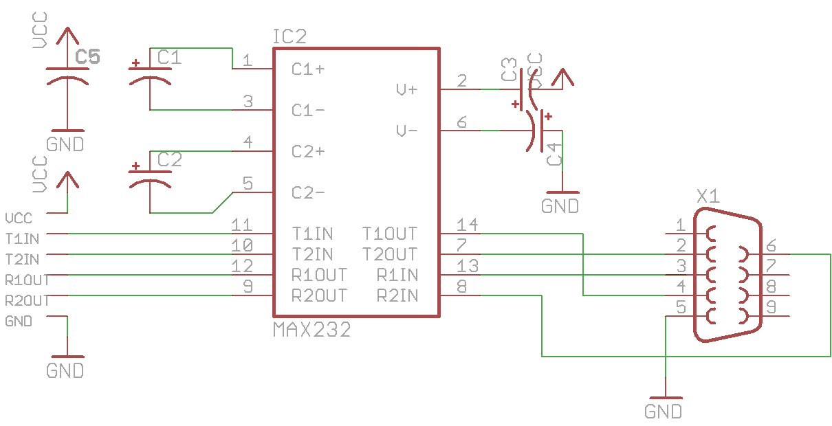
Pin 16, VCC should be given 5V directly. There should be a decoupling capacitor C4 between VCC and Ground.
I can never remember which way round TX and RX is relative to, so I made sure I could jumper them to reverse the signals. I think I've got RX (Arduino) pin connected to 11 on the MAX232.
Westfw's schematic is pretty much how you'd want to hook it up. Except that the schematic uses both of the recieve and transmit lines of the max232. You don't need to do that if all you want is one serial line. The max232 supports two complete serial lines. You just use R1 and T1. On a 9 pin serial line that's pins 2 and 3 (with 5 being the ground.) For simple RS232 serial those are the only three pins that need to be hooked up. This means that in this schematic you'd be using T2 and R1 which is confusing but won't hurt anything.
So if you want one TTL to serial connection then follow that schematic but don't hook up the connections to the DB9 pins 4 and 6.
Oh, and you asked why a connection from VCC to ground is needed. It's for noise suppression. Digital ICs tend to be noisy and they also tend to send some of that noise back through their power input. With lots of ICs all in the same circuit they can and will send interference to each other. This interference will do strange and hard to diagnose things to the functioning of the circuit. You do not want this at all. This is where our friend the decoupling capacitor comes in. It suppresses the noise on the power pin. In short, use them. You will thank yourself later.
[quoteexplain to me what the arrowing at the end of V+ pin mean[/quote]
In order to avoid cluttering schematics with wires to the power supplies, it is common to use a common symbol to indicate "this is connected to the common gnd", or "this is connected to the common +5V", or whatever. All of these are "invisibly" connected (or treated as the same connection, because they enforce the same "net" name.) The arrows you see are a somewhat common symbol designed to show this connection. You might also note that the max232 symbol I used (which is from one of the standard eagle libs) doesn't have power supply pins shown on the schematic. These are also "invisible" and automatically connected to the like-named net.
In (large) professional schematics, it's pretty common to reserve an entire page for nothing but the bypass caps.
Actually, in large professional schematics it's pretty common for each signal to come off a pin to some sort of named arrow, with no actual drawing to show where its connected to, which can be pretty annoying (but I don't know how else you handled 100+ pin chips without making a mess...)
Thank you very much. This has been very informative. How would you "invisibly" connect a wire to the common ground in eagle?
There are standard eagle libraries "supply1.lbr" and "supply2.lbr" that contain assorted symbols and signal names. (the actual "arrow" components I used.) When you attached them to a net, it names the net to the appropriate signal name, and all nets with the same signal name are connected whether there is a wire drawn between them or not. (this also means you can draw a short net connected to a pin and use the "name" command to connect that piece of wire to the net with the same name.)
There are standard eagle libraries "supply1.lbr" and "supply2.lbr" that contain assorted symbols and signal names. (the actual "arrow" components I used.) When you attached them to a net, it names the net to the appropriate signal name, and all nets with the same signal name are connected whether there is a wire drawn between them or not. (this also means you can draw a short net connected to a pin and use the "name" command to connect that piece of wire to the net with the same name.)
Thank you very much for this. You have been very helpful. I will re-design the schematics and then post up again for a check.
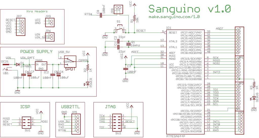
I have tried MAX232 (as in datasheet), connected to ATMEGA328 Rx, Tx and also Reset PINS (DTR resets with 100n capacitor). Works fine with USB / RS 232 convertor. Behaves exactly like native Arduino board - sketch upload and serial communication is ok.
I have tried MAX232 (as in datasheet), connected to ATMEGA328 Rx, Tx and also Reset PINS (DTR resets with 100n capacitor). Works fine with USB / RS 232 convertor. Behaves exactly like native Arduino board - sketch upload and serial communication is ok.
Can you provide me the schematics on how you did that?
First get Arduino schematic from http://arduino.cc/en/uploads/Main/arduino-duemilanove-schematic.pdf. Remove FTDI chip related part, the rest is ok (I mean Xtal, 22 pF cond, LED ...).
Connect MAX 232 as on the attached schematic - it seems I am unable to attach JPG file I try to send it as email.
There is a bug on your schematic : DTR on RS232 is pin 4, not pin 7.
The rest seems to be ok.
10k + 100n is for reseting the Arduino - see original Duemilanove schematic. When Arduino IDE uploads a sketch, it resets Arduino using DTR pin. A bootloader starts after reset and communicates through Rx / Tx pins with computer which sends the sketch.
I have checked the sanguino on http://farm4.static.flickr.com/3292/2696504917_df57af371c_b.jpg. It contains 10k resistor and 100n capacitor already. So simply use MAX232 as on your schematic without 10k + 10n and connect it directly to the reset on sanguino. Close jumper JP8 and use USB2TTL conector. I am not sure, if sanguino uses RTS or DTR - try it.