MCP23S17-E/SP - Arduinio Uno R4 Wifi - Test

I am working on a project that will use a grid of 24x24 Hall Effect sensors. A3144

To do this I will need to use multiplexing and one option to avoid solder and labor of 10k ohm resitors was to purchase MCP23S17. vs CD74HC4067 (which will require 10k resitor per HED).

So cost of chip more is well worth avoiding labor in soldering 500 resisors. But testing with even basic structure I am not making progress.

/ ┌────────┐

// GPB0(1) │● ○│ (28) VDD (+5V)

// GPB1(2) │ │ (27) VSS (GND)

// GPB2(3) │ │ (26) RESET

// GPB3(4) │ │ (25) A2

// GPB4(5) │ │ (24) A1

// GPB5(6) │ │ (23) A0

// GPB6(7) │ │ (22) INTA

// GPB7(8) │ │ (21) INTB

// NC(9) │ │ (20) CS

// NC(10) │ │ (19) SCK

// GPA7(11)│ │ (18) SI (MOSI)

// GPA6(12)│ │ (17) SO (MISO)

// GPA5(13)│ │ (16) GPA0

// GPA4(14)│ │ (15) GPA1

// └────────┘

I have even rulled out the HED and KISS to pin 1 (withi dot). Ground or +5v


#include <SPI.h>
#include <Adafruit_MCP23X17.h>

Adafruit_MCP23X17 mcp;

const int mcpCS = 2;     // MCP CS → D2
const int testPin = 0;   // GPB0 (MCP pin 1)

void setup() {
  Serial.begin(115200);
  SPI.begin(); // Uses D13, D11, D12

  if (!mcp.begin_SPI(mcpCS)) {
    Serial.println("MCP init failed");
    while (true);
  }
  Serial.println("MCP initialized");

  // Configure GPB0 as input with pull-up
  mcp.pinMode(testPin, INPUT);
  mcp.digitalWrite(testPin, HIGH); // Enable pull-up
}

void loop() {
  bool pinState = mcp.digitalRead(testPin);

  Serial.print("GPB0 voltage level: ");
  Serial.println(pinState ? "HIGH (+5V)" : "LOW (GND)");

  delay(500);
}

But serial output ( reset button to capture new state). During test I move pin from ground to +5v but it no change.


20:11:07.576 -> MCP initialized
20:11:07.576 -> GPB0 voltage level: LOW (GND)
20:11:08.069 -> GPB0 voltage level: LOW (GND)
20:11:08.562 -> GPB0 voltage level: LOW (GND)
20:11:09.088 -> GPB0 voltage level: LOW (GND)
20:11:09.582 -> GPB0 voltage level: LOW (GND)
20:11:10.076 -> GPB0 voltage level: LOW (GND)
20:11:10.571 -> GPB0 voltage level: LOW (GND)
20:11:11.097 -> GPB0 voltage level: LOW (GND)

This is same if I have pin 1 (GPB0) connected to nothing, to ground, or to +5v.

But then I find other sites where diagrams show:


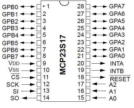
I tried both. but same result. I know this chip is “packaged” multiple ways” but WHY the pins are different ?!!?!?

Question:

  1. Silkscreen on chip is MCP23S17-E/SP (I purchased 30 of them). Does anyone have some experience with these mux chips with Arduinio Uno R4 Wifi?

  2. Any recommendations on how to debug? I figured if I KISS to just Ground vs +5 it would prove out chip logic, but then went down rabbit whole of chip pin layout.

Post an annotated schematic showing how you have wired it. Have you read the data sheet?

https://www.microchip.com/en-us/product/MCP23S17

Thanks for reponse. I think I made some progress. I also joined chat session with MicroChip and person in chat was very responsive and helpful. She confirmed image/ pin out which means this video: https://www.youtube.com/watch?v=Q_ZC1-RZPdk. SHOULD be correct and so I configured it to be the same.
test to match what is in this youtube video: https://www.youtube.com/watch?v=Q_ZC1-RZPdk. ping 14 MISO D12, pin 13 MOSI to D11, pin 12 SCK to D13, pin 11 CS/SS to D10. Pin 10 to ground, pin 9 to +5v DC. Pins 15-17 which are A0-A2 are all to ground denoting this as chip ID 000. the pin 1 whichi is GPB0 is unplugged but I need to test ground vs +5 v.

#include <SPI.h>
#include <Adafruit_MCP23X17.h>

Adafruit_MCP23X17 mcp;

const uint8_t CS_PIN = 10;  // Chip Select
const uint8_t TEST_PIN = 8; // GPB0 = pin 1 on MCP23S17

void setup() {
  Serial.begin(115200);
  while (!Serial) delay(10);

  SPI.begin();  // Initializes SCK, MOSI, MISO
  if (!mcp.begin_SPI(CS_PIN)) {
    Serial.println("MCP23S17 not found. Check wiring.");
    while (1);
  }

  // Set GPB0 as input
  mcp.pinMode(TEST_PIN, INPUT);

  Serial.println("MCP23S17 initialized. Monitoring GPB0...");
}

void loop() {
  int val = mcp.digitalRead(TEST_PIN);
  Serial.print("GPB0 (pin 1) reads: ");
  Serial.println(val ? "HIGH (+5V)" : "LOW (GND)");
  delay(500);
}

Serial output unplugged

08:12:42.363 -> GPB0 (pin 1) reads: HIGH (+5V)
08:12:42.856 -> GPB0 (pin 1) reads: LOW (GND)
08:12:43.383 -> GPB0 (pin 1) reads: LOW (GND)
08:12:43.877 -> GPB0 (pin 1) reads: LOW (GND)
08:12:44.371 -> GPB0 (pin 1) reads: HIGH (+5V)
08:12:44.865 -> GPB0 (pin 1) reads: HIGH (+5V)
08:12:45.393 -> GPB0 (pin 1) reads: HIGH (+5V)
08:12:45.887 -> GPB0 (pin 1) reads: LOW (GND)
08:12:46.382 -> GPB0 (pin 1) reads: LOW (GND)
08:12:46.876 -> GPB0 (pin 1) reads: LOW (GND)
08:12:47.404 -> GPB0 (pin 1) reads: HIGH (+5V)
08:12:47.898 -> GPB0 (pin 1) reads: HIGH (+5V)

Serial output when GPB0 plugged into ground

08:13:18.032 -> GPB0 (pin 1) reads: LOW (GND)
08:13:18.562 -> GPB0 (pin 1) reads: LOW (GND)
08:13:19.056 -> GPB0 (pin 1) reads: LOW (GND)
08:13:19.551 -> GPB0 (pin 1) reads: LOW (GND)
08:13:20.044 -> GPB0 (pin 1) reads: LOW (GND)
08:13:20.573 -> GPB0 (pin 1) reads: LOW (GND)
08:13:21.062 -> GPB0 (pin 1) reads: LOW (GND)
08:13:21.555 -> GPB0 (pin 1) reads: LOW (GND)
08:13:22.081 -> GPB0 (pin 1) reads: LOW (GND)

Serial output when plugged into +5v


8:14:02.288 -> GPB0 (pin 1) reads: HIGH (+5V)
08:14:02.780 -> GPB0 (pin 1) reads: HIGH (+5V)
08:14:03.271 -> GPB0 (pin 1) reads: HIGH (+5V)
08:14:03.796 -> GPB0 (pin 1) reads: HIGH (+5V)
08:14:04.291 -> GPB0 (pin 1) reads: HIGH (+5V)
08:14:04.783 -> GPB0 (pin 1) reads: HIGH (+5V)
08:14:05.277 -> GPB0 (pin 1) reads: HIGH (+5V)
08:14:05.804 -> GPB0 (pin 1) reads: HIGH (+5V)

So I think I have wire logic down, and some basics sitched up. Now in bread board I have A3144

Digital output to GPB0.

#include <SPI.h>
#include <Adafruit_MCP23X17.h>

Adafruit_MCP23X17 mcp;

const uint8_t CS_PIN = 10;     // Chip Select for MCP23S17
const uint8_t SENSOR_PIN = 8;  // GPB0 = pin 1 on MCP23S17

void setup() {
  Serial.begin(115200);
  while (!Serial) delay(10);

  SPI.begin();  // Initializes SCK, MOSI, MISO
  if (!mcp.begin_SPI(CS_PIN)) {
    Serial.println("MCP23S17 not found. Check wiring.");
    while (1);
  }

  // Set GPB0 as input and enable internal pull-up
  mcp.pinMode(SENSOR_PIN, INPUT);
  mcp.digitalWrite(SENSOR_PIN, HIGH);  // Enables pull-up resistor

  Serial.println("MCP23S17 ready. Monitoring A3144 sensor on GPB0...");
}

void loop() {
  int sensorState = mcp.digitalRead(SENSOR_PIN);
  Serial.print("A3144 Sensor: ");
  Serial.println(sensorState ? "NO MAGNET" : "MAGNET DETECTED");
  delay(250);
}

when no magnet around serial is

08:22:05.335 -> A3144 Sensor: MAGNET DETECTED
08:22:05.560 -> A3144 Sensor: NO MAGNET
08:22:05.825 -> A3144 Sensor: NO MAGNET
08:22:06.089 -> A3144 Sensor: NO MAGNET
08:22:06.320 -> A3144 Sensor: MAGNET DETECTED
08:22:06.584 -> A3144 Sensor: MAGNET DETECTED
08:22:06.815 -> A3144 Sensor: MAGNET DETECTED
08:22:07.079 -> A3144 Sensor: MAGNET DETECTED
08:22:07.343 -> A3144 Sensor: NO MAGNET
08:22:07.573 -> A3144 Sensor: NO MAGNET
08:22:07.837 -> A3144 Sensor: NO MAGNET

with magnet

08:22:39.387 -> A3144 Sensor: MAGNET DETECTED
08:22:39.616 -> A3144 Sensor: MAGNET DETECTED
08:22:39.880 -> A3144 Sensor: MAGNET DETECTED
08:22:40.144 -> A3144 Sensor: MAGNET DETECTED
08:22:40.373 -> A3144 Sensor: MAGNET DETECTED
08:22:40.635 -> A3144 Sensor: MAGNET DETECTED
08:22:40.900 -> A3144 Sensor: MAGNET DETECTED
08:22:41.129 -> A3144 Sensor: MAGNET DETECTED
08:22:41.393 -> A3144 Sensor: MAGNET DETECTED

I add in 10k ohm resitor from HGED digital read pin to +5v pin and it works “as expected”.

I was really hoping , and per guide I read to use these MCP23S17-E which could do auto pull up, and avoid the extra soldering and complexity of the resitor. Alternative was /is CD74HC4067. which must have these but is even more soldering. This board is one of many and at 500+ HED, it makes a difference.

Yes but only one per IC

thx for response but you note “one per IC”. do you mean one 10k ohm resitor per CD74HC4067 that would shift this quite a bit.

Yes. You only need one on the common pin not one for each of the IO pins. Make sense?

Sorry.. I guess I am not following. For each HES string (up to sixteen per CD74HC4067) I see logic for common “rail” for power and ground. But when each digital signal pin goes to pin on the MUX chip, how would you be able to use a common 10k ohm resitor.

I am newbie on chip / board layout.. still learning tricks and means to do this efficiently.

Since you can only select one of the 16 at a time you only need one 10K pull-up on the sig pin. Sig pin (pin 1) in the TI 4067 data sheet it's called common

I think i track logic. the “sig” pin, or “com” pin .. which is different one chip vs another ( and I am finding that documentation is not the best when a chip is put in different ‘packaging’ and so pin layouts differ :stuck_out_tongue: ) The SIG/COMMON pin is a means for you to use a common pullup for your inputs.

In the case of MCP23S17-MC

I think.. this is pin 11. noted as CS.

On CD74HC4067

Seems its the one labled “SIG”

And its pullup is against ground as its baseline.. would link to ground. But that part I am not sure on.

No to 5V. You also connect sig to an arduino pin.

So if a magnet is present it will read LOW.
If no magnet it will read HIGH.

I get you on +5v via 10k ohm resistor.

I am not quite following the “connect to arduino” pin. What is the function or code snip, that is needed or helps this work. Do I need to use Analog pin to read in the pull up “level” such that it has baseline to read input signal as it scans? Or is this more about digital pin that there is baseline of voltate for reading signal? What is the code snip I guess. What is the ROI for giving up a pin.

Appreciate your wisdom and input.

I assume you want to read the state of the hall sensor with the arduino so you need to connect it to the arduino. Any digital pin will do.

ROI, what is that?

I think it's time to explain what your project is all about.

ROI - Return on Investment

AKA: I am pushing the pin count on the Arduino UNO R4 Wifi and its clock scan times to its limit.

As for what I am doing.. a lot.. I never do anything easy :slight_smile:

This is one of ten board games I am building: T02 → which is a simple game structure but one of the more complex in solding and setup on arduino. The game is a grid of 24 x 24 color change LEDs. In a grid. Then each board will have sub games:

t0201a → go

t0202a → connect4

t0203a → tic-tac-toe

t0204a –> color game( simple color select and draw on board)

You can choose to play pvp or pv AI. I am starting with t0203a as that is the simplest.

I have LED logic done, wifi , player logic, game libraries (start game, score, leds, OLED display for game state etc..). I now need to bind logic of for each LED on grid will be corresponding HED.

so I need 576 HED to sense magnets and then use function to “play” game with that input.

so with each board having Color change LED (for main board state track), OLED display (game score/ time left etc) and then two digital pins for the two WS2812B led strips. The rest of the pins I can allocate for HED. These games for t02 are slower read, but need to also accomodate where game read of HED may need to read fast. Sorry.. thats a lot. And thx

For the 32 muxes, you will need 32 pins for sigs and 4 pins for S0...S3 so that's 37 pins. You will have to either add another level of muxes (mux the 32 muxes) or use another board like the mega2560 that has more pins.

Befor you go down another rabbit hole, you might consider using a different hall switch, one that has a push-pull output that will work with the MCP23S17

I have purchased 16 x CD74HC4067. I have 40 MCP23S17-E

On paper: 8 x MUX per 4 pins into arduinio. each mux would be 128 HES.

### 🔗 Shared SPI Bus (All MCP23S17 Chips)
- D11 → MOSI (Master Out Slave In)
- D12 → MISO (Master In Slave Out)
- D13 → SCK  (SPI Clock)

### 🧩 Chip Select (CS) per Chain
- D2  → CS for Chain A (MCP0–MCP7)
- D3  → CS for Chain B (MCP8–MCP15)
- D4  → CS for Chain C (MCP16–MCP23)

### 🧲 RGB LED Control
- D5  → Red Channel
- D6  → Green Channel
- D7  → Blue Channel

### 🖥️ OLED Display (I²C)
- A4  → SDA
- A5  → SCL

### 🛠️ Reserved / Expansion
- D8–D10 → Available for interrupts, diagnostics, or future CS lines
- A0–A3  → Available for analog reads or expansion

### 🧠 MCP23S17 Addressing (Per Chip)
- Pins 15–17 (A0–A2) on each MCP23S17 define its hardware address:
  - GND = 0, NC = 1
  - Example: MCP0 → A0=A1=A2=GND → Address 0
             MCP1 → A0=NC, A1=A2=GND → Address 4
             MCP2 → A0=GND, A1=NC, A2=GND → Address 2

Now I am open to suggestions. But that was the plan. I am now past “plan” into.. test with mux units reading the HES… and no plan survives the breadboard test….

If what you are calling an HES is the hall sensor, then there are 16 per 4067 mux not 128. You will need 32 hc4067s. As I said you will need 32 pins for the sig inputs and 4 more for the S0,S1,S2,S3 connections. That's 36 pin total.

Or you can take the 32 sig outputs and go into two more muxes. Now you have 2 pins for the sig inputs and 8 pins for the select pins (S0...S3). However scanning all the inputs might be slow.

If I stick with the MCP23S17 I think each chain of 8 which will cover 128 Hall Effect Sensors (HES)

Diagram only shows two chains but five chains will then consume 16 Digital pins (D2-17). This will then leave OLED to use SLC/SDA. And the two LED chains to be D0-D1 LED strips.

I thought you said it did not work with the MCP23S17 when using the internal pullup.
The internal pull-up on that IC is rather large, typical 66K ohms. Even if you do more breadboard testing you may have noise problems in your final design.

and that diagram is wrong.

Are you making a PCB for this?