I've had a custom Mega2560 based board built. I've basically followed Mr Nick Gammons examples in the design, here and now I'm trying to get the boot loader in. However, at the board detector stage, I'm failing to detect the board.
Again, I'm following Mr Gammons examples and using his Board Detector Sketch using a spare Arduino Mega2560 clone I have.
I've got the boards connected using pins 50 - 53 (changed these values in the code to match)...
Pin 50 - MISO
Pin 51 - MOSI
Pin 52 - SCK
Pin 53 - Reset
I get the "Failed to enter ICSP programming mode. Double check wiring" message.
I've double checked the wiring A LOT!
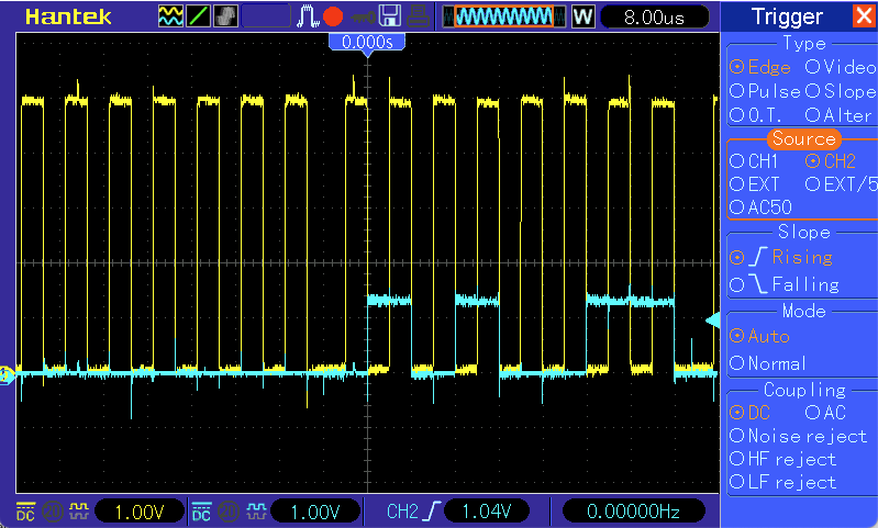
I've tried to test various signals with an oscilloscope. I think I have 5v and 0v in the right places. I can see the MOSI signal bopping away and also the SCK. However, I can't see anything on the MISO.
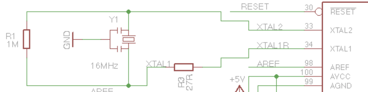
I've got a crystal on the board, but I don't know how to check if it's working. I've tried using the board detector sketches clock on pin 9, but it doesn't seem to be doing anything - I couldn't see how it was working in the code either.
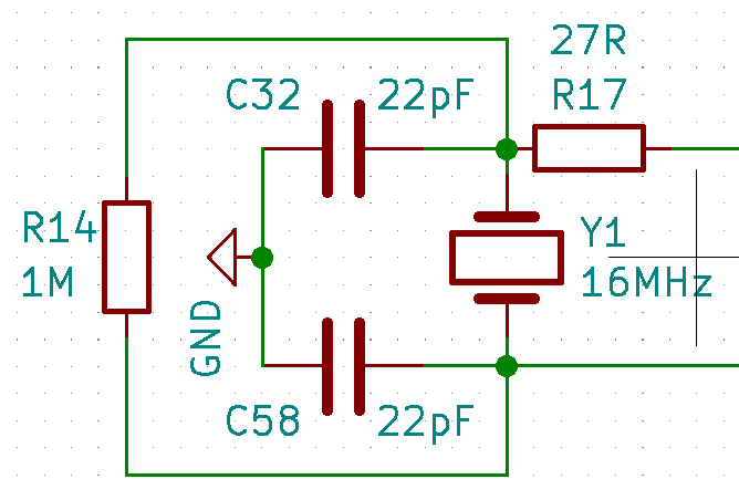
Scope XTAL2. Why is there a parallel resistor in your xtal circuit? Do you have a true quartz crystal, or a resonator? I'm not sure but isn't 22pF kind of small for the reset circuit?
If the target 2560 is a virgin device, then I believe that it comes out of the factory configured to use the internal oscillator. If that's the case, then initially you don't need to worry about your external crystal. The target device should still be detected.
Might be worth showing the whole schematic of the target board.
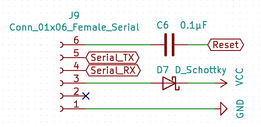
The official Mega schematic has this capacitor. I'm not sure what its purpose is. The essential auto-reset capacitor is a different one: C7 on the official schematic.
The crystal is a ECS-160-12-33Q-JEN-TR - data sheet here. Perhaps the caps may be slightly off now I've read into it a bit more.
I put the resistors in the crystal circuit purely because I saw it in the Arduino schematic. Probably not the best way to design a circuit, admittedly.
I've tried scoping XTAL2, but I'm not sure on what I'm looking for. What amplitude should I expect? Should it look like a nice obvious reasonably square pulse? - I certainly haven't found one of these. The best I've been able to see, I can only describe a ripple at about 450mv, and it looks to be unstable. I'm a novice, so it's likely my scope settings are off - I've just tried looking at a bunch of different timebases at 1v per division amplitude. Probes are at x10. I'll try to get a screenshot later.
You're right re the reset capacitor; I got it from the Arduino schematic. I also do have the C7 one...
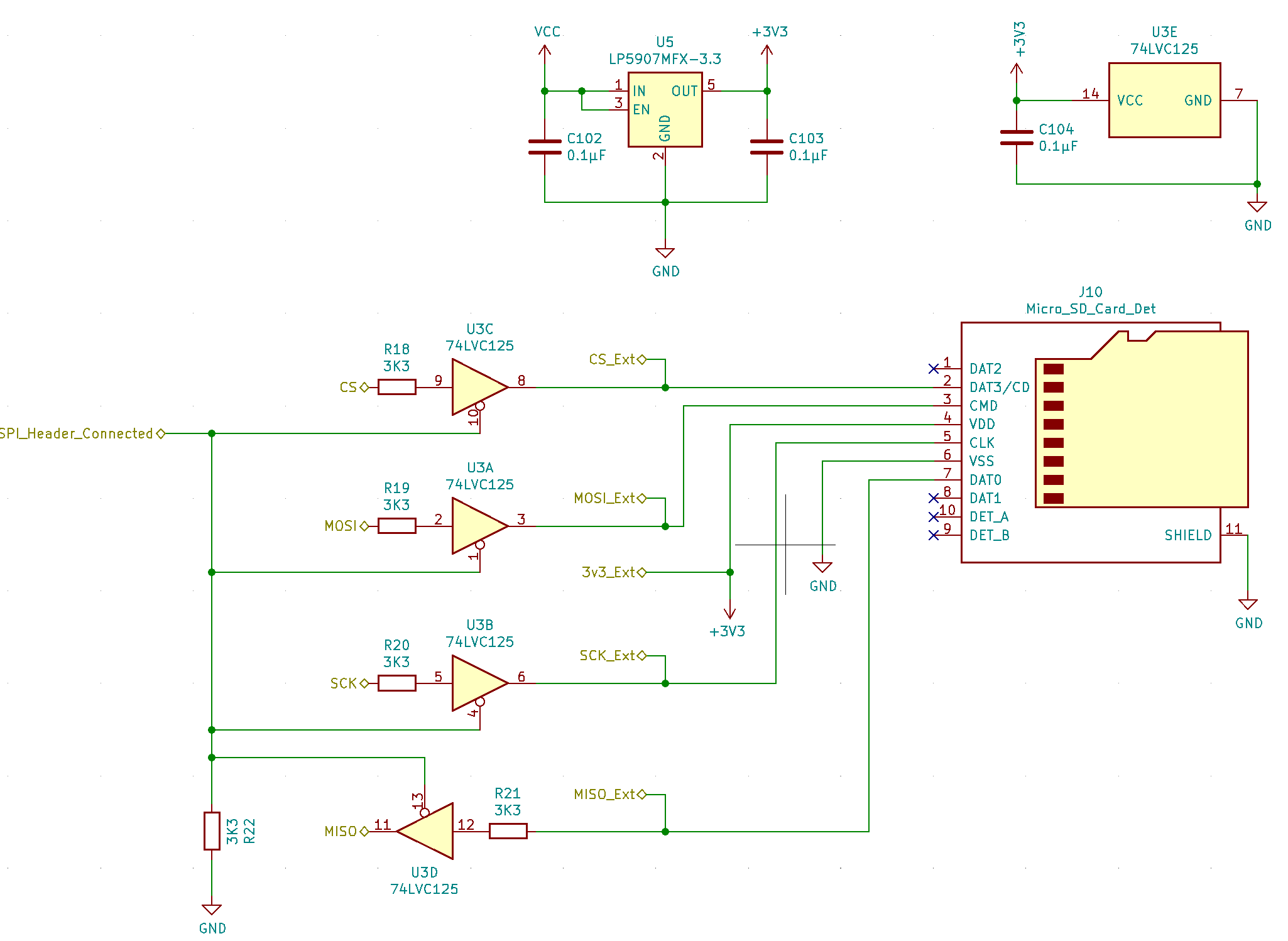
I'm trying to use an SD card as well (currently none inserted) and I'm using the 74LVC125 as a level shifter and also to allow a future hex loader function (also based on Mr Gammons example). The main board will use the SD card normally, and a separate board will be plugged in and use the SD card for uploading the hex file. This is a problem for future me to worry about, assuming it's not this bit of the circuit that's the problem.
Thanks for the link. Regarding the layout, my capacitors aren't as suggested there. They are all grouped together near pin 26 (see original post for image). Will this be major problem?
It is a factory fresh chip, so this gave me a ray of light, but I still haven't got any board detected. I found the following bit of code I think is what you are talking about...
#if USE_BIT_BANGED_SPI
  digitalWrite (MSPIM_SCK, LOW);
  pinMode (MSPIM_SCK, OUTPUT);
  pinMode (BB_MOSI, OUTPUT);
#else
  digitalWrite (RESET, HIGH);  // ensure SS stays high for now
  SPI.begin ();
  SPI.setClockDivider (SPI_CLOCK_DIV64);
  pinMode (SCK, OUTPUT);
#endif  // (not) USE_BIT_BANGED_SPI
Is it the SPI_CLOCK_DIV64 what sets the frequency? Would dividing 16 MHz by 64 not give 250 KHz anyway, or doesn't it work that way? In any case I tried changing it to SPI_CLOCK_DIV128, and still no cigar.
Can you expand on this a bit. Are the pin numbers referring to the 2560 acting as the programmer, and the signal names referring to the pins on the custom 2560 board?
In Mr Gammons board detect sketch, it was based on an UNO. I've changed the RESET variable from pin 9 to pin 53 (and the wiring to suit). I'm not using Bit Banging, so I think it should be good to go like that.
The oscillator circuit on the Mega is for a resonator. The device you linked to is a quartz crystal. The 1M resistor doesn't belong there, also the 27 ohm is a random addition that should go. I'm more concerned about a lack of pi network capacitors (because the schematic component for a resonator may show them built in, but they may not be on the board, am I right?). On other quartz circuits, you'll see a pair of 10-22 pF capacitors on the two sides of the crystal. Those are necessary for stability.
As far as measurements, you won't see any activity at the clock oscillator pins until you enable the external oscillator in software via the config register.
I'll certainly ditch these on my next board. Thanks.
Sorry, not sure I follow completely with pi caps... The two caps and the two resistors on my schematics around the crystal are on the board. Is this what you mean
Right, OK. So crystal issues aside, I should be able to get the board recognised with its default internal clock of 1 MHz, and get a boot loader in. So there's still something fishy with my setup.
So am I correct in saying it is responding, but the amplitude is too low? When I look at the MOSI signal it's up at 5v -ish, matching the SCK amplitude.
Purely out of curiosity, which schematic is that? I haven't seen something like your R17 before. I'm just a little interested in understanding more about it.
Capacitors are not an exact science. There are some general best practices such as what is recommended on that schematic, and then there is what you can get away with, which might even go all the way to leaving caps out entirely if you are lucky and not concerned with reliability. I have seen some professional PCBs where the caps were a fair distance away from the chip they provide decoupling for. Likely there were manufacturability considerations that influenced that placement and the engineer determined that it was safe to place them there even though not ideal.
All that is a long winded way of saying: "I don't know".
This resistor is the feedback register of the crystal oscillator circuit.
If you want to know more about this resistor,
please googling "crystal oscillator feedback register".
EDIT:
p.s.
It is often unnecessary for the oscillator circuit built into the microcontroller.
If you make your own CMOS oscillator circuit, you should add it.
I've made some progress with this, but hit another wall.
Like I said in an earlier post, I've got this part of the circuit which is intended to allow the board to use an SD card, and also in the future allow another board to be connected and use the SD card / SPI to load a Hex file to the processor. So I have the 74LVC125 to shift the voltage levels and also allow the SPI to be isolated. I had a thought that the MISO signal was being pulled low because the enable signal on the 74LVC125 was low and there is no SD card connected. So I stuck 5v on the enable, giving the MISO output on U3D pin 11 high Z.
So all happy, I tried the chip programmer sketch and got this...
10:04:34.972 -> Atmega chip programmer.
10:04:34.972 -> Written by Nick Gammon.
10:04:34.972 -> Version 1.38
10:04:34.972 -> Compiled on Sep 21 2021 at 10:04:25 with Arduino IDE 10813.
10:04:34.972 -> Attempting to enter ICSP programming mode ...
10:04:35.078 -> Entered programming mode OK.
10:04:35.115 -> Signature = 0x1E 0x98 0x01
10:04:35.115 -> Processor = ATmega2560
10:04:35.115 -> Flash memory size = 262144 bytes.
10:04:35.115 -> LFuse = 0x62
10:04:35.115 -> HFuse = 0x99
10:04:35.115 -> EFuse = 0xFF
10:04:35.115 -> Lock byte = 0xFF
10:04:35.115 -> Clock calibration = 0x52
10:04:35.115 -> Bootloader address = 0x3E000
10:04:35.115 -> Bootloader length = 7474 bytes.
10:04:35.115 -> Type 'Q' to quit, 'V' to verify, or 'G' to program the chip with the bootloader ...
10:05:07.021 -> Clearing 'Divide clock by 8' fuse bit.
10:05:07.021 -> Fixing low fuse setting ...
10:05:08.018 -> Programming mode off.
10:05:08.018 -> Attempting to enter ICSP programming mode ......................................................
10:05:14.390 -> Failed to enter programming mode. Double-check wiring!
10:05:14.390 -> Programming mode off.
10:05:14.390 -> Type 'C' when ready to continue with another chip ...
So to me it looks like it did something, but it looks different to what I was expecting from the guide on Mr Gammons website. And now there is again no response from the chip. This time, the MISO signal is always high, and the MOSI is always low. I do still get the SCK pulse, as before.