Hello,
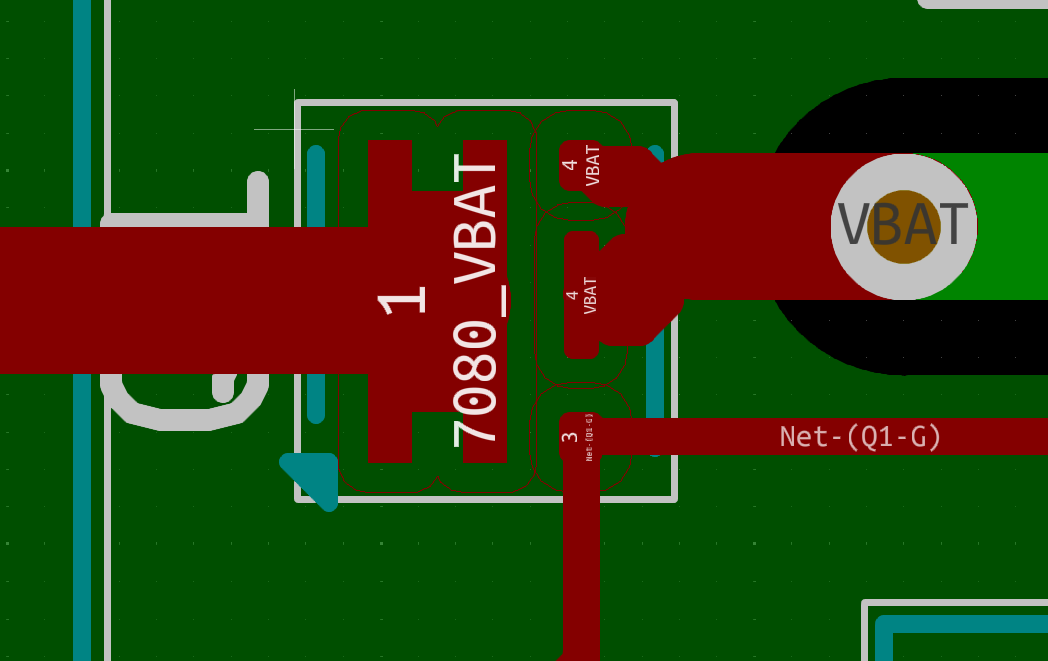
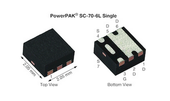
Does anybody know why is PowerPAK SC70-6 Source terminal connection is a little weird? Why is it split into two parts?

How should I route it / them?

Thanks in advance.
Hello,
Does anybody know why is PowerPAK SC70-6 Source terminal connection is a little weird? Why is it split into two parts?
How should I route it / them?
Thanks in advance.
For heat dissipation.
Be careful you that don’t connect the Drain and Source under the chip.
I understand that regarding the drain terminal, which is much bigger area than the two source terminals combined. But the Source, especially the small separated PIN 4? I don't think so.
Be careful you that don’t connect the Drain and Source under the chip.
Luckily KiCad would not allow me to do that anyway.
Something looks inverted to me between the package diagram and the footprint. Is red the upper copper layer and is that a 'top' view of the package?
I see it now. That perspective drawing makes an interesting optical illusion. I thought it was a "see through" top view when I first saw it. That could have unpleasant consequences if you're designing a footprint.
I agree, it's a bit tricky.
I believe the datasheet would have the final word on this topic.
You mean about the routing for this particular MOSFET?
Unfortunately, I didn't find any relevant info there: SiA445EDJ.
I think the cleanest way to do this Kicad is create a small zone around the pads, with clearance set to 0. Hopefully that creates a solid fill and keeps DRC happy.
I couldn't find any reference designs using this package. Also, might be worth asking on forum.kicad.info
Found these at Kicads community contribution page:
Use symbol SiA449DJ
Vishay_PowerPAK_SC70-6L_Single
This topic was automatically closed 180 days after the last reply. New replies are no longer allowed.