PCB for Multiplexer Layout

That looks fine to me.

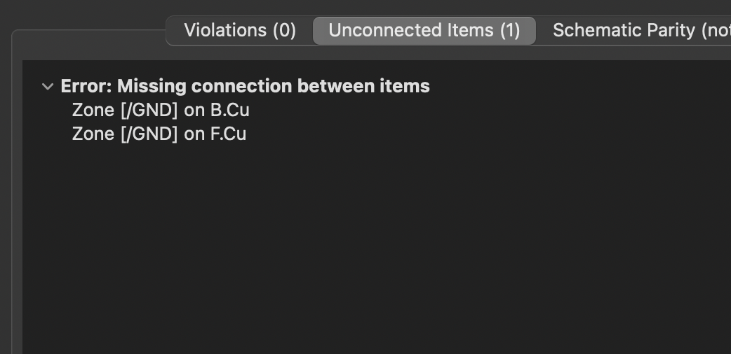
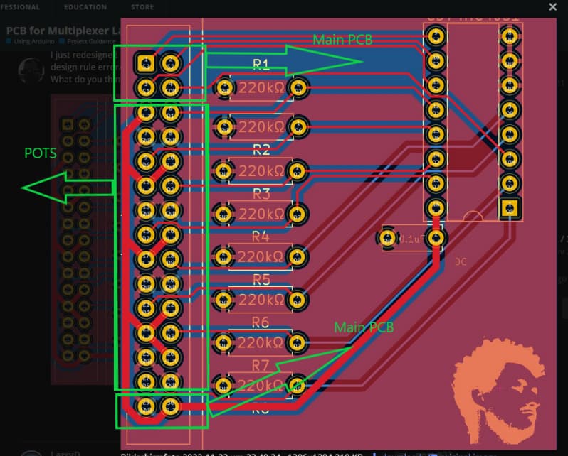
This is not something I am expert in, others here might want to comment on what I say, the ground plane is not just there to provide a convenient connection for everything, it also provides a low impedance path for ground. Note 'ground' does not equal negative, a common misunderstanding with beginners. Ground is often connected to negative but can just as easily be the positive of the supply or the middle, for example with a -15V, 0V +15V supply often used for analogue audio. Anyway, I digress. Having a plane provides a low impedance path for signals and power, much better than a track does. It also provides some level of noise shielding and it provides for high frequencies to have a return path that corresponds to the route of the track that carries the signal (which you don't need to worry about for the frequencies you are working with). There is a general rule in electrical circuits that you need to keep the current in both directions in adjacent wires to minimise noise pick up. A cable with all the wires bound together isn't just neat and tidy it also allows the signal and it's return to be kept together, which is essential for noise reduction. A ground plane does the same on a PCB because each track will be adjacent to the ground wherever it goes. As for a supply plane on the other side, I think the same argument applies, but I defer to the knowledge of others if someone wants to comment.

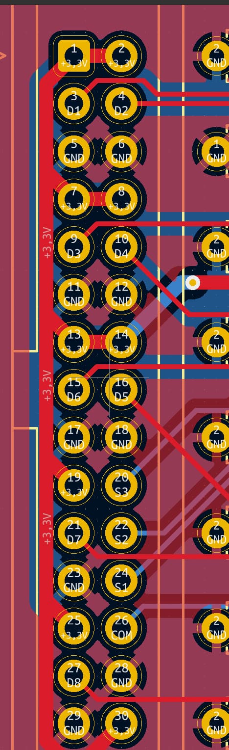
So, to translate the general comment above into something practical for your project, although the frequencies you are dealing with are low (varying voltage from adjusting a pot), the noise frequencies also have to be dealt with, and these are higher. Your circuit needs to minimise noise pick up. You need to consider the wider context of how it will be connected to its 8 pots, how it will be connected to power and how it will be connected to whatever micro-controller / Arduino you are using. The 2 connectors @6v6gt suggested makes sense. The wires to the pots should in in one cable, neatly routed and with the wires broken out to the pots as they go past. I suggest a 10 way connector and cable, that's 8 signals, 0V and +3V3. It should look neat when completed, not just for aesthetic reasons but because neat generally translates to low noise pick up.

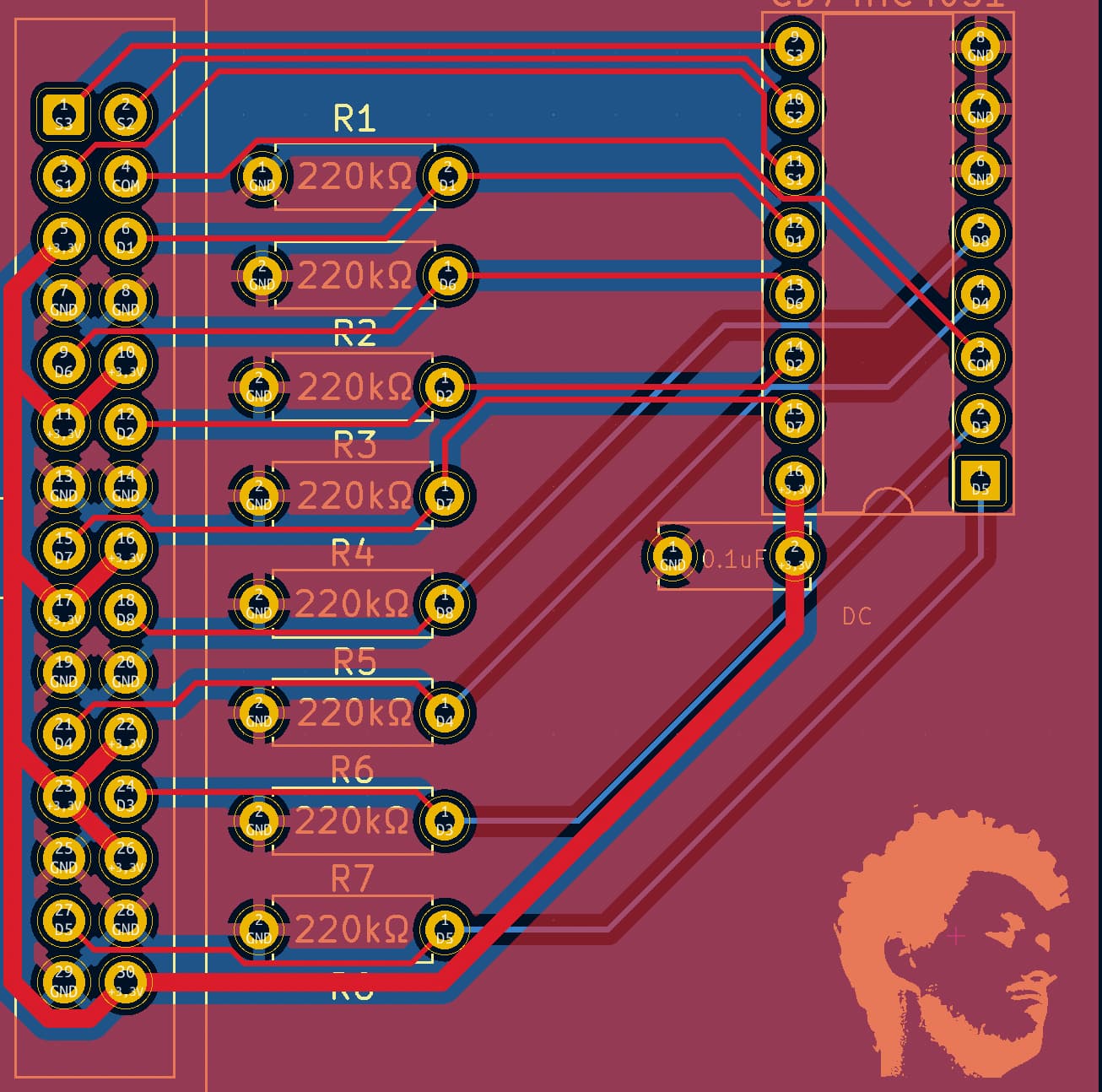
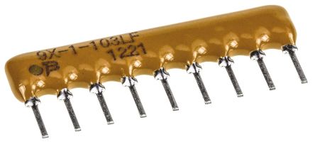
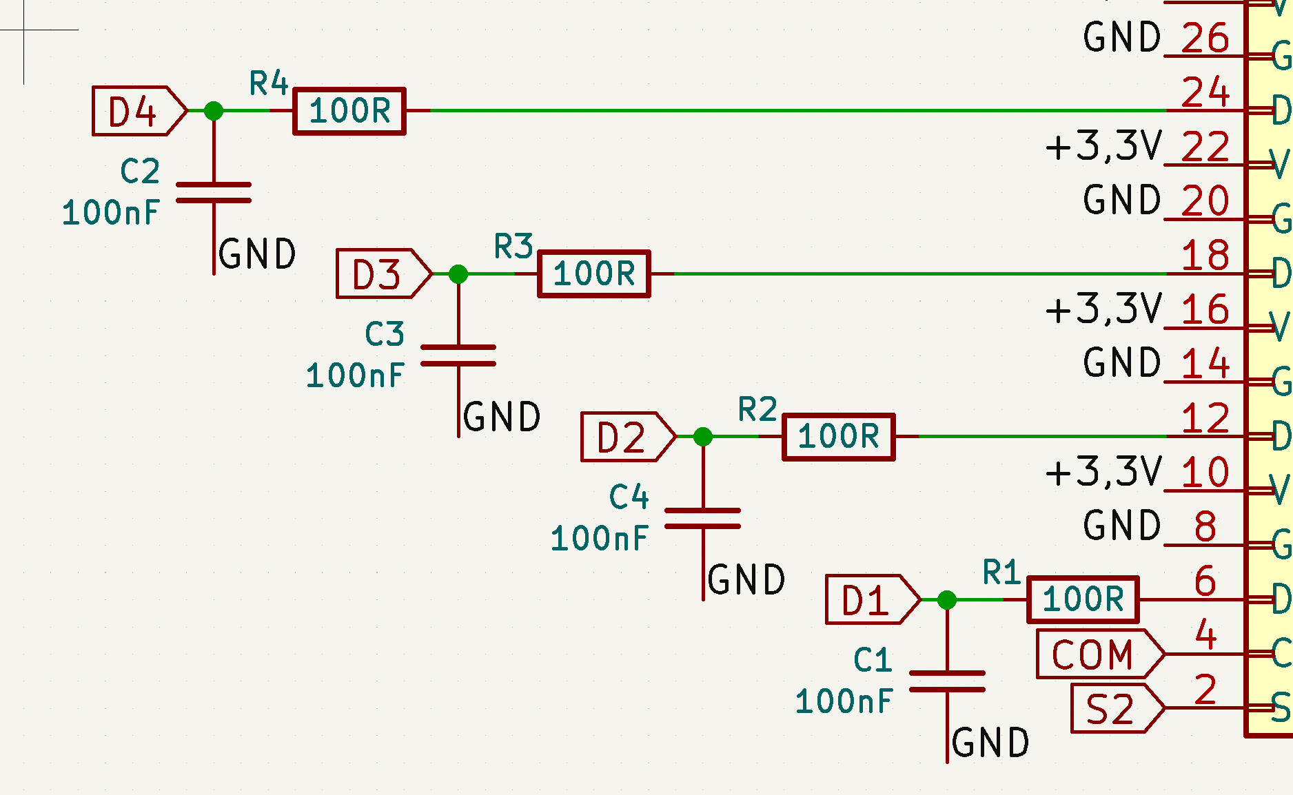
As others have said, the capacitor on pin 16 should be 0μ1 ceramic for decoupling of the power to the chip.

Mike's advice on the input filter is good, if you have a problem with unstable readings on the input to your A2D then deal with that in software. I would expect them to vary by at least plus and minus 1 anyway, however carefully you design the electronics.

Yes because that is the nature of an A/D converter. What ever you do you can't get more consistent than that. When you are dealing with MIDI the range you use is 0 to 127, so the readings from the A/D in the 0 to 1023 range will have to be divided by four anyway.

In a MIDI system you usually introduce some sort of hysteresis, so that it ignores small movements before you go for the divide by four.

@PerryBebbington
@6v6gt
Thank you so much for your kind replies! I'll think about the layout you both recommended. My idea behind the 30 pin connector was that every cable I need on the PCB arrives at this single connector. 8 signal cables for the potentiometers, 8 poti power cables, 8 poti gnd cables, 3 Mux Serial In, 3 Mux Serial Out and 1 communication pin also for the multiplexer.
I thought that's neat too :smiley:

@Grumpy_Mike
Thats exactly what I did, I have hysteresis in my code and the values are very stable.

I didn't realise that your plan was separate power and 0V for each pot. In that case they should be next to each other on the connector, with the signal wire in the middle. So: 0V, signal, 3V3 repeat etc. If you do that then 3 wires from the connector to each pot, with the 3 kept together in one cable, not separated. You could use ribbon cable and split the wires out 3 at a time next to the pot they go to. The important thing is to keep the 3 together, whether they are close to other groups of 3 is not important. The reason is as per my other reply, it reduces noise pick up, resulting in more stable readings. I would probably put a 0μ1 ceramic capacitor close to the connector as well for decoupling.

Edit
Maybe
0V, Sig, 3V3, 3V3, Sig, 0V etc

Why? They all have the same voltage on them, always. The current is quite low.

Alright, thats good to know because I didnt plan to group them this way.
I have at the moment all the data pins next to each other and every 3.3v and 0v pin in the second row. No grouping at all.

And I have 0v, data and 3.3v cables for each potentiometer because this way I could change potentiometers faster if something doesnt work. Is it maybe not a good idea? Should I simply wire all the gnd and 3.3v pins together on the potis and only connect the data wires to the PCB?

I just redesigned the PCB using your advices. I still sticked to the 30pin connector but kept the potentiometer wire groups together. What do you think?

I just figured out that this error occours because I created a power plane island somewhere but i just can't find it. I would appreciate every hint. :smiley: Thank you!

The Kicad design rules check normally leaves tiny yellow arrows where there is a problem.
Also clicking on the error message tends to bring the problem area into focus.

The suggestion I made in reply #24 doesn't work because it doesn't take account of the order the wires connect to the connector. Sorry for the mistake but you will need to design the board again.

Check this against a connector:

0V, 3V3, Sig
Sig, 3V3, 0V

You need to end up with the wires something like:
0V, Sig, 3V3, 3V3, Sig, 0V, 0V, Sig, 3V3...

@6v6gt
Alright, I will check that later! thank you:)

@PerryBebbington
Oh, now I get it! Thats a neat idea indeed​:smile: No worries, i will redesign it later and post a picture of the new version. Thank you for your help! :slight_smile:

I just redesigned it the way you suggested and it looks the best to me and also it doesn't have any design rule error/warning.
What do you think about it?

Do yourself a huge favour and use a SIP resistor network.

image

image

Your wiring layout could probably be better consolidated to avoid cable groups going to different destinations :

You could also add a couple of vias in the bare area on the front copper layer around the R1 label.
What about mounting holes or is that just the way you have cropped the image ?

@Grumpy_Mike

I thought about using capacitors like in one of the first pictures I've attached, because the frequency of the value change of the potentiometer is going to be pretty low. (it's going to be tweaked with my hands, so nothing really fast)
By using a pull down resistor, all I'd get is the value dropping down to 0 whenever there is a small moment of floating inside the potentiometer or not? By using the capacitor I'd basically have a "sample and hold" method to save values for a short period of time to avoid any random jumps. What do you think?

@6v6gt
You are totally right, thank you so much for pointing that out! I'll edit the layout and upload it as soon as I'm done. :slight_smile:

You can change the the pot quite fast even by hand.

Yes but there is no reason for a pot to do this, unless it is faulty.

Yes you would, but you would not get the DC value to help with the cross talk unless all of the pots are connected on the multiplexer.

But at the end of the day it is your choice.

Did you check against a connector? I didn't when I made the suggestion and it is possible it is mirrored along the long axis if I made a mistake. I don't have time to check now, but please make extra sure it's right.

Following on from @6v6gt's suggestion on reply 34 I would use 2 connectors, one for the link to the main PCB and one for the pots. Also consider how multiple boards will be connected to each other.

@Grumpy_Mike

"yes you would, but you would not get the DC value to help with the cross talk unless all of the pots are connected on the multiplexer."

Sorry i don't fully understand it. Could you please explain it a little bit more in detail?

By crosstalk you mean that one of the values which gets sent by tweaking the pot changes the value of the one sitting next to it?
And just to make sure, you mean by DC value the decoupling cap value, right? :smiley:

Also please if you have good resources for these topics, I'd love to read them.
I know, the internet is full with these things, but I'm sure you know some gold nuggets. :slight_smile:

@PerryBebbington
What do you exactly mean by the mirroring along the axis? Everything seems to me to be fine. I'm going to upload a new picture though, as soon as I'm done, because I changed some things back.

My idea behind only one connector was that it's less complicated and for the serial wires, I planned to use a long ribbon cable, which I can cascade by clipping headers on it wherever I have a Multiplexer PCB.
Also I thought that it's always better to have every incoming cable in one place instead of splitting it to two or three different ones.
For the communication pin and power and ground cable I could also simply stick to the 30 pin connector and just split the ribbon cable partially.
Another reason was simply the fact, that I couldn't find all the different components in Germany with similiar specs like same pitch for example.
I mean, at the end of the day, it doesn't count, but I'd still love to use 2.54mm for every connector so that I don't have to keep that in my mind.

If you both suggest me though, that it's a better idea to split it, I'd switch to that and re-design the PCB.
Then, I'd even take three instead of two connectors:
24pins for the pots
6 serial (3in, 3out in order to cascade it) - used between the multiplexer PCBs
3 to the main board - 1 ground, 1 power, 1 multiplexer communication pin

What do you think about this? :slight_smile:

Have you looked at using a SIP resistor network ?

Yes I did, but I thought it's only relevant if I'd do it the way how GrumpyMike suggested it, by not using capacitors. This way, it makes sense to me to use the SIP resistor network, but I thought that you can't connect it if you have it between data pin and the connector. (see attached picture) This way, every resistor would need two individual legs and not one which is always connected to a common ground.
It's a really good idea though, if I'd stick to the version without the capacitors and using an SIP resistor network only as pulldowns.
Or did I misunderstand it? Please correct me if I'm wrong.