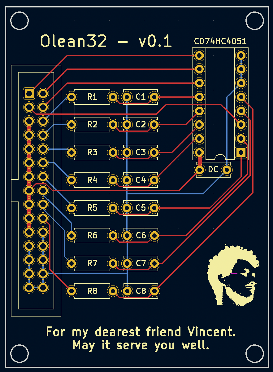
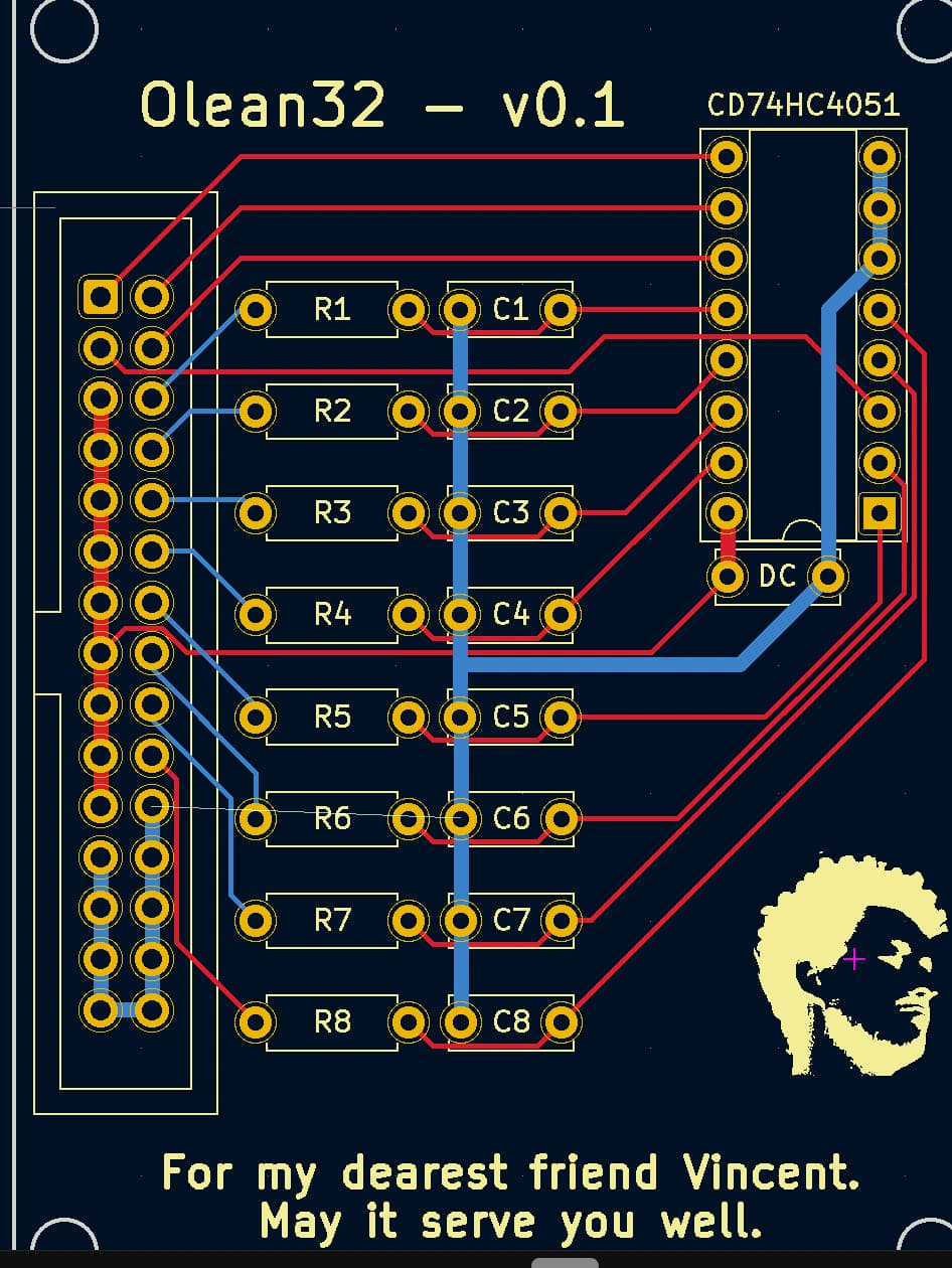
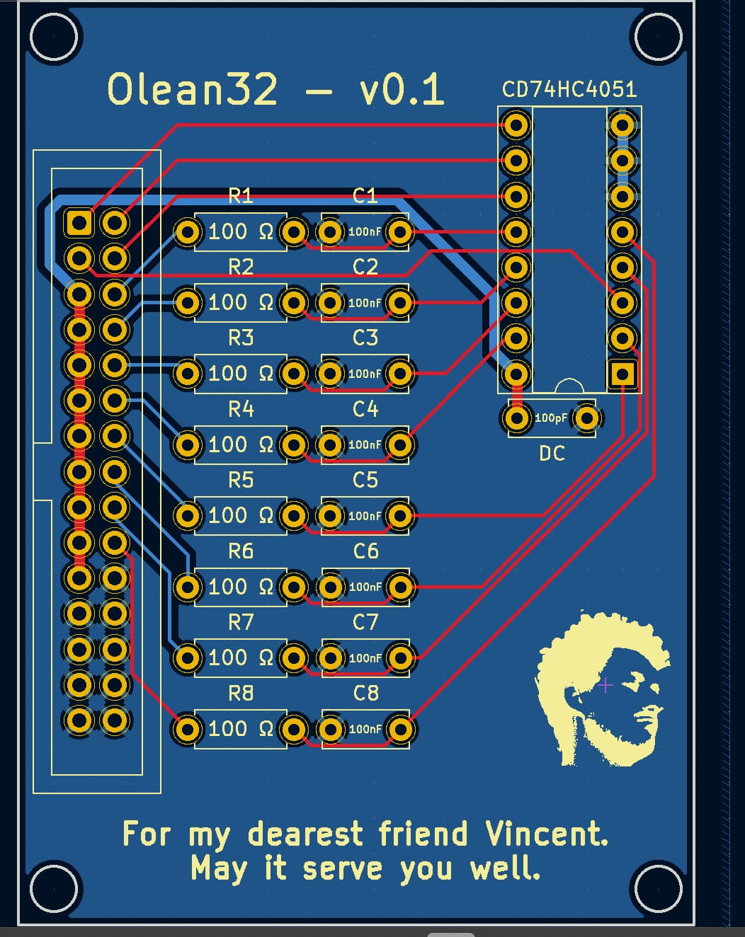
I'm relatively new to KiCAD, but I finally created my first PCB Layout. I want to use it as a part of a MIDI controller with 32 potentiometers. My plan is to cascade four of these PCBs in order to get the values of all of the potis. The heart of it is going to be a Multiplexer which I'm going to feed through the 2x15 IDC cable. The PCBs are all going to get connected to a main PCB which has a Teensy on it. Do you maybe have any critic or observations which I maybe overlooked?
If not, then it's time to order those PCBs!
Also I'd be happy about good tips on where to order these! I thought about jlcpcb. (I live in Germany)
I'd be grateful about every helpful comment.
I changed the width to 30mils for the power traces except for the decoupling capacitor, due to place issues. Is it still okay or would it be an important part to also change that one?
It's called a "pour" in ECAD. Check the KiCad docs.
You can find ground plane examples everywhere. Probably 98% of digital boards have them. You made some of the traces thicker, but you missed the connection to the pin header. Actually, where is any ground connection to the header? I only see a net wire. I can't see perfectly but it looks like the header to circuit power trace is still thin.
You have to decide, whether you want to just make something one or two times and move on, or you want to really learn how to do it well.
[soapbox]
You have purchased a blank PCB, loaded with copper.
You are paying someone to remove that copper, which you purchased.
They are not giving you a discount for the copper they reclaim.
You have plenty of room so keep YOUR copper and use it to help provide strong solder points and good gnd and current carrying capacity.
[/soapbox]
@anon57585045
I just made all the power and ground traces thicker (30 mils)
@TomGeorge
Thank you for the advice Tom. I made the power and ground traces thicker as aarg already suggested it but making it even thicker would cause a lot of routing problems and also I saw many people use this thickness for all the data traces. If you could provide me some good reasons though, why it's better to have it even thicker, I'd consider redoing the PCB.
@PerryBebbington
Thank you, just did it! Hope thats correct this way.
I see everywhere that they also create ground plane on the top layer but what is the reason for that? Isn't it enough to have it at the bottom so that every element which has to get connected to GND has a short path to it?
Also, could I just use GND for the bottom and my power (5v) rail for the top layer? Or is there a reason for having GND on both sides. This way I'd have even less tracks.
@Grumpy_Mike
to be honest, I began this project earlier and read about filters and came to the conclusion or maybe just found it somewhere in the internet, that 0.1 uF should be fine. I couldn't give you a proper argument. Thank you for reminding me though, I'm going to read about it more, especially if you say that it's not a good value to use.
I am saying that a filter of any sort on the input to a multiplexer is a very bad idea because it limits the frequency of any signal you are trying to put through it.
If I was designing this then I would remove the 100R resistors altogether and replace all the capacitors with something like a 220K resistor to prevent pickup and reduce cross talk in the multiplexer.
But then it is not my project, maybe you have a reason for doing this?
I think I understand you now. So you mean by that that it's not going to register any high frequency changes regardless of the components I'd take for the filter? It'd make it basically react slow to everything?
I tested it out by soldering it on perfboards and it works just fine, but my goal is to build a proper device not just something what happens to work.
My only reason for using filters was to filter out any random jitter, which works pretty well.
It may sound stupid, but does the method you recommend me with the 220k resistor have any name which I could use to read about it? Or maybe you could explain me the basic physics behind it, why that should work..
Have I got this right? These 32 potentiometers are not carrying any audio signals. You are simply polling an analog value (voltage 0 to 3.3 volts) from these from time to time to control another device. If that is the case, at what frequency are you polling these potentiometers and what is their value (ohms) ?
Ahh, pull down resistance! That makes sense now. Very interesting, especially because it'd not just improve the circuit but also reduce the size of the PCB.
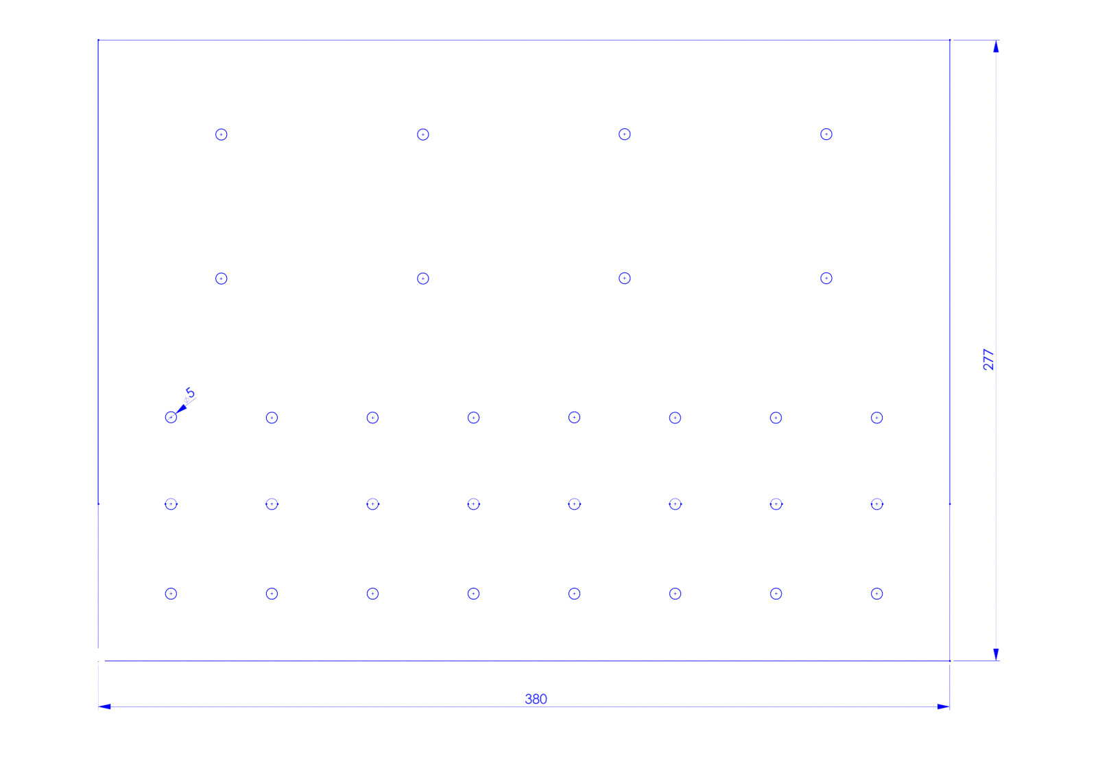
How are you going to group the components? For example, are all 32 potentiometers going to be in the same box or have you 4 boxes each with 8 potentiometers ?
I'd probably have considered having two connectors on each board. One for the potentiometer group and one for the multiplexer control, common and power going to the main PCB but I guess that depends on how you are laying it all out.
This is the layout of the potentiometers. I planned to have one PCB for every 2 potentiometers at the top and 6 at the bottom.
This way I could evenly space them.