I cut that down to an hour:

3 Likes
I'm sure that all that advice about rescuing your 6-layer EMI-non-conformant boards by adding another couple of layers, on your designs with 400+ ball BGAs (where 100+ balls are power) is going to be highly relevant to the sorts of things we do here. (I didn't see ANYTHING in there about 2-layer boards...)
2 Likes
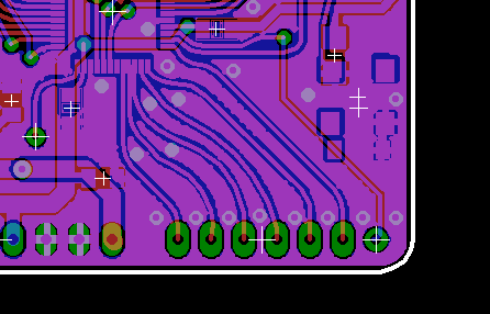
The PCB I am working on is only 2-sided proto-board. I took everyones advice and put the ground plane on the backside of PCB. I have never soldered a PCB with vias in contacts before. I have heard of doing that in the past but, I didn't take it seriously until now. I put a power plane on the front side as well. Bonus, I was able to reduce the design by a couple of millimeters by doing the contact vias. ![]()
I will post the project once I debug the PCBs.
Notable quotes in that video:
Electricity is the same thing as light. The difference is their frequency.
Guy was worried about getting solder in the vias... the teacher said that he didn't care if it was peanut butter. It doesn't matter.
Electricity doesn't follow the traces, it follows the plastic.
Be careful with vias in pads. I generally either have a very short trace or a pour on pads that extend past the pad and put the vias there. Vias in pads can lead to tombstoning components, the solder likes to pull through the via to the ground plane and not leave enough for a good connection on the pad.
Mind you, it can be done, just be careful.
I did it both ways because some of my contacts were too small for vias.
- A power plain is not necessary, power traces are fine.
I did it in addition because I couldn't find a route for a trace.
That reminds me of another quote from the video: "You pay for the material removed from the layers, not added."
-
With modern PCB manufacturing techniques, balancing copper on layers or leaving copper on the top layer is not necessary and does not change PCB cost.
-
The important thing for you, the designer, is to have an unbroken GND plane on the bottom, any traces on the bottom should be short and strapped so return ground signals do not need the hunt for a return path the GND.
-
Let’s see your latest design to be sent to the manufacturer.
-
Now to be clear, these are indeed best practice guide lines. There are 10s of thousands of PCBs poorly routed that still function well.
No no no. It is not about that.
There are huge theory part. He discuss return paths, analog/digital parts placement and many many other. I found it very interesting :). He explains why having big ground planes or making whole chassis to be ground sometimes makes things worse. Worth to watch, at least 1st half of the video.
He makes very simple examples, slowly advancing to more complex topics.
And this is one of the most important. He mean that energy is transferred through the plastic between signal and ground. All that area, where energy flows, must be free of other signal traces. Or you’ll get interference.
Then your layout may be bad. If you can't connect two points with a trace, then a copper pour will also not work.
Using copper pours for power can be misleading since it may contain long and/or very narrow copper paths that can't handle the current
I did add a trace with a lot of vias to connect the smaller islands. Just to get the whole ground plane grounded.
It doesn't impact the price of the proto-board. But, It looks like a lot of extra stuff.

and probably useless and unnecessary.
A ground or power plane is one layer of solid unbroken copper.
What you are doing is just connecting nets using a copper pour.
If you can't lay out a single-sided board, you probably can't lay out a board with a "ground plane of solid unbroken copper."
And your whole board doesn't need a ground plane - if you can get relatively unbroken copper under your high frequency areas that are more susceptible to noise, you'll be doing better than most...
because I couldn't find a route for a trace.
That's a bad sign, though. If you couldn't route a ground trace, it probably means that your ground pour is following a really convoluted path...
1 Like

The islands are being created by two connectors sharing circuits.
My original question was how to deal with the dead islands:
A: Connected islands with complete ground plane (first image).
B: Deleted islands (2nd image black area).
C: Dead islands (3rd image non glowing gray area).
BTW, those are three different configurations of the rear ground plane.
You guys are leaning towards the "B" answer... deleted dead islands.
I did this "ground-planed and sort-of shielded" area for the analog area of an Arduino-like board. It seemed like a reasonable idea. I haven't done any testing that would show it better or worse than other solutions, EMI or noise -wise.

So, those are vias connecting each other? With a trace or a plane connecting each other?
I did a simular version in my image A (2 posts ago).
Can you show a schematic diagram for your project ? It appears to be little more that a 14 pin IC with a number of alternative headers/connection pads.
Yeah; ground fill/"trace", connect with vias to the ground plane on the other side of the board...
You might want to also note that I am not now, nor have I ever been, a "professional" PCB designer.
I was thinking the same. It might make it less "noisy" and maybe some EMI protection.